
Introduction
With the demand for improving power efficiency and extending the operating time of battery-powered devices, the ability to analyze power loss and optimize power supply efficiency is more critical than ever before. One of the key factors in efficiency is the loss in switching devices.
This application note will provide a quick overview of these measurements and some tips for making better, more repeatable measurements with oscilloscopes and probes.
A typical switch-mode power supply might have an efficiency of about 87%, meaning that 13% of the input power is dissipated within the power supply, mostly as waste heat.Of this loss, a significant portion is dissipated in the switching devices, usually MOSFETs or IGBTs.
Ideally, the switching device is either "on" or "off" like a light switch, and instantaneously switches between these states.In the "on" state, the impedance of the switch is zero and no power is dissipated in the switch, no matter how much current is flowing through it. In the "off" state, the impedance of the switch is infinite and zero current is flowing, so no power is dissipated.
In practice, some power is dissipated during the "on" (conduction) state, and, often, significantly more power is dissipated during the transitions between "on" and "off" (turn-off) and between "off" and "on" (turn-on).
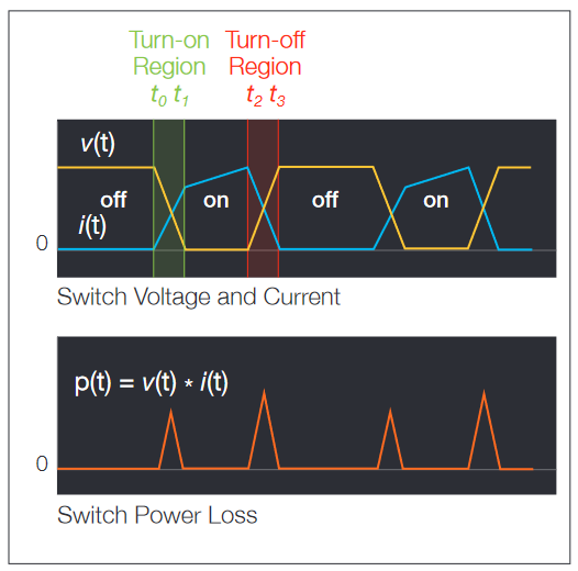
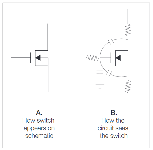
These non-deal behaviors occur because of parasitic elements in the circuit. As shown in Figure 3b, the parasitic capacitances on the gate slow down the switching speed of the device, extending the turn-on and turn-off times.The parasitic resistances between the MOSFET drain and source dissipate power whenever drain current is flowing.
Conduction Loss
In the conduction state, the switch does have a small resistance and voltage drop across it, and the switch dissipates power as a function of the current flowing through it.
For a MOSFET, this power is typically modeled as:
P = ID2 * RDSon = ID * VDS
- where ID is the Drain current,
- RDSon is the dynamic on-resistance between the Drain and the Source, often < 1 W, and
- VDS is the saturation voltage between the Drain and the Source, often < 1 V
For an IGBT or BJT, this power is typically modeled as:
P = IC * VCEsat
- where IC is the Collector current and
- VCEsat is the saturation voltage between the Collector and the Emitter, often < 1 V
Turn-on Loss
During turn-on, the current through the switch rapidly increases and the voltage drop across the device quickly decreases. However, parasitic elements, such as the Gate-to-Drain capacitance in a MOSFET, prevent the switch from turning on instantaneously. While the device is turning on, there is significant current flowing through the device and significant voltage across the device, and significant power loss occurs.
For a MOSFET, during turn-on, this power is typically modeled as:
P = ID * VDS
- where ID is the Drain current and
- VDS is the voltage between the Drain and the Source
For an IGBT or BJT, during turn-on, this power is typically modeled as:
P = IC * VCE
- where IC is the Collector current and
- VCE is the Collector to Emitter voltage
Turn-off Loss
In a similar manner, during turn-off, the current through the switch rapidly decreases and the voltage drop across the device quickly increases, but circuit parasitics prevent the switch from turning off instantaneously. While the device is turning off, there is significant current flowing through the device and significant voltage across the device, and significant power loss occurs. The equations above also apply.
Measuring Switching Loss
There are two approaches to measuring switching loss: it can be measured using manual setups and built-in oscilloscope measurements, but there are also automated measurement systems available on some oscilloscopes. The automated measurements have the advantages of being easy to set up and delivering easily repeatable results. With either technique, careful probing and optimization will help you get good results.
Probing and Measurement Setup
Before discussing the specific power measurements, there are six key steps to making accurate and repeatable measurements:
1. Remove voltage offset errors: The amplifiers in differential probes may have a slight DC voltage offset which will affect measurement accuracy. With the inputs shorted and no signals applied, automatically or manually adjust the DC offsets in the probe to zero.
2. Remove current offset errors: Current probes may also exhibit DC offset errors due to residual magnetism in probe, as well as amplifier offsets. With the jaws closed and no signals applied, automatically or manually null out the DC offsets in the probe.
3. Remove timing errors: Because instantaneous power measurements are calculated based on multiple signals, it is important that the signals be properly time-aligned. Different technologies are used to measure voltages and currents, and the propagation delays through these devices may be significantly different, leading to measurement errors. Good results are generally possible by adjusting the inter-channel timing to account for the difference in nominal propagation delays in the deskew menu. For the most accurate results, apply a high-slew-rate signal to all inputs and carefully remove any relative timing offset (skew) between all channels.
4. Optimizing Signal-to-Noise Ratio: In all measurement systems, but especially in digital devices such as modern oscilloscopes, good measurement technique requires keeping signals as large as possible (without clipping) to minimize the effects of noise and to maximize vertical resolution. This includes using the lowest necessary attenuation when probing the signals and using the full dynamic range of the oscilloscope.
5. Signal conditioning: Measurement quality can also be improved by conditioning the input signals. Bandwidth limiting can be used to selectively reduce noise above the frequencies of interest, and averaging can be used to reduce uncorrelated or random noise on the signal. High Res acquisition mode provides bandwidth limiting and noise reduction, increased vertical resolution, and it even works on signals acquired in single shot mode.
6. Accuracy and safety: For best accuracy, be sure to use the equipment within the normal operating range and below the peak ratings. And, for your safety, always stay well within the equipment’s absolute maximum specifications and follow manufacturer's instructions for use.
Measuring Switch Loss - Manual Setup and Built-in Measurements
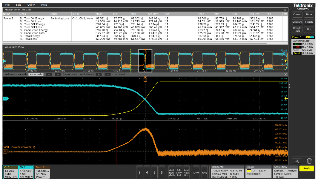
One way to measure turn-off loss is with gated measurements. The object is to measure the average power dissipated during the turn-off phase. In this example, the MOSFET's VDS is acquired with a differential voltage probe and is shown in yellow in Figure 4. The Drain current is acquired with an AC/DC current probe and is shown in cyan. The vertical sensitivity and offset of each channel is adjusted so the signals occupy more than half of the vertical range, but without extending beyond the top and bottom of the graticule.
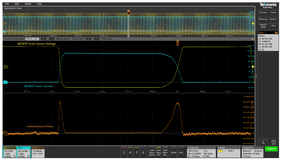
A stable display is important for visual analysis, so the oscilloscope’s edge trigger is set to the 50% point on the voltage waveform. Then the sample rate is set to assure adequate timing resolution on the signals edges. In this case, a sample rate of 6.25 GS/s results in many sample points on each edge of the switching waveform. Finally, High Res acquisition mode is enabled to increase the vertical resolution to 16 bits.
Waveform math is then used to multiply the current by the voltage to create the orange instantaneous power waveform.An automated measurement is used to measure the average or mean value of the power waveform.
In this example, the engineer manually adjusted the oscilloscope to optimize the quality of the switching loss measurement. At a later date, this engineer or another engineer would likely set up the measurement slightly differently, resulting in different measurement results.Automating the measurement through power analysis software removes many of the sources of variation.
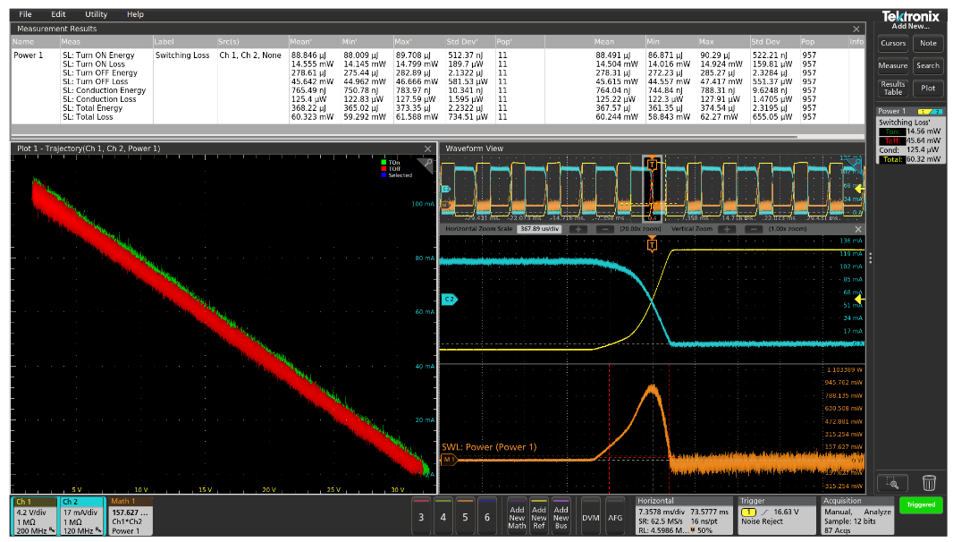
Measuring Switch Loss - Automated Using Power Analysis Software
To consistently optimize the setup and improve measurement repeatability, a power measurement application can be useful. In this case, the PWR Advanced Power Analysis application provides a custom autoset for the Switching Loss measurement and then, with the push of a button, makes the full suite of switching loss power and energy measurements.
Slew Rate and Switching Loss
As expected from inspecting the instantaneous power waveform and as indicated by the switching loss measurement values in Figure 5, the turn-off loss is the dominant loss mechanism in the total switching loss. A potential cause of this high loss is the performance of the switch drive circuit. If the transition time or slew rate of the drive signal is slower than expected, the switch will remain between on and off states longer than expected, and the switching losses will be higher than expected.
A slew rate measurement is the change of voltage in a given time interval (usually between the 10% and 90% points on an edge) and has the units of volts/second. Because the mathematical derivative is inherently a high-pass filter, and thus will accentuate noise, it is recommended that you use averaging to reduce the effects of random noise on these measurements.
Slew rate measurements can be made manually with cursors by placing one waveform cursor at the 10% point of the signal edge and the other cursor at the 90% of the waveform edge. The slew rate is then calculated by dividing the difference between the voltage measurements by the time difference between the cursors. This technique requires the user to estimate the 10% and 90% points on the waveform and calculate the result.
Many oscilloscopes can improve this process with automatic measurements. Automated amplitude and rise-time measurements can be used to determine the amplitude of the signal, set the measurement threshold values at 10% and 90% of that amplitude, and then measure the rise-time of the signal. And, in the case of a complex signal, cursor gating can be used to focus the measurement on a specific portion of the waveform. Then the slew rate is then calculated by multiplying the amplitude by 80% and dividing by the rise-time measurement.
However, power analysis software makes slew rate measurement setup easy, and it reduces variation in measurement results as the design engineer adjusts component values in the circuit.
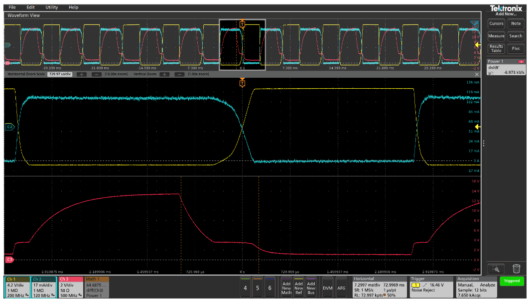
A cursor-gated slew rate measurement on the MOSFET gate (VGS, shown in red on channel 3 in Figure 7) shows that the switching signal was much slower than the design spec, because of higher-than-expected capacitance at the gate of the switching device.
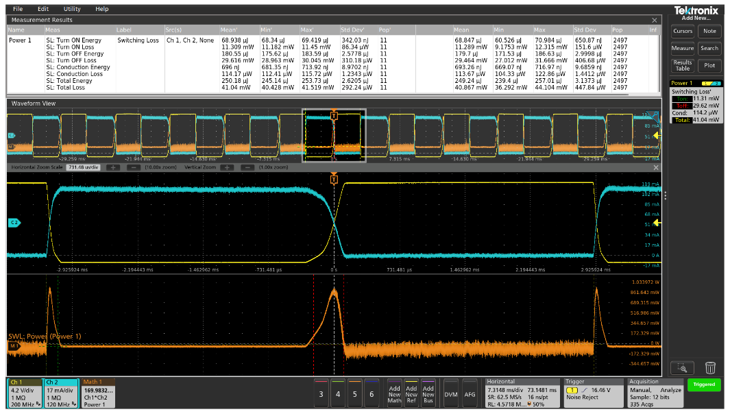
The exponential decay, shown between the vertical cursors in Figure 7, is a function of the output impedance of the gate drive circuit, the parasitic gate capacitances within the switching MOSFET device, and the circuit board capacitances at the gate. When the speed of the drive signal was increased, by reducing the gate drive output impedance and the capacitance at the gate node, the switching loss was improved by almost 30%, as shown in Figure 8.
Switching loss measurements are a critical part of optimizing the efficiency of switch mode power supplies. By using good measurement techniques and automating the power measurements, it is easy make a series of complex switching loss measurements, quickly and repeatably
Find more valuable resources at TEK.COM
Copyright © Tektronix. All rights reserved. Tektronix products are covered by U.S. and foreign patents, issued and pending. Information in this publication supersedes that in all previously published material. Specification and price change privileges reserved. TEKTRONIX and TEK are registered trademarks of Tektronix, Inc. All other trade names referenced are the service marks, trademarks or registered trademarks of their respective companies.
09/19 46W-60010-3


