When a high performance system or component needs to be verified, it often requires attaching an oscilloscope probe.For high speed circuits, the effect of attaching a probe often cannot be ignored.
This application note covers a range of topics and challenges, such as circuit loading, simulation of probe effects, the impact of connecting with long wires, and single-ended and differential measurements with a TriMode™ probe. These topics relate to today’s complex high performance circuits and will help users of performance probes maximize the signal fidelity of their measurements.
Probe Loading Basics
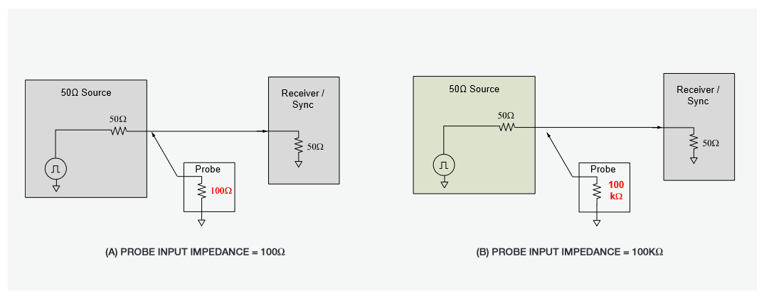
When a probe is attached to a circuit, it is important to understand the probe’s impact on the circuit’s behavior. The degree of probe loading depends upon two factors: the input impedance of the probe and the sensitivity of the circuit to this impedance. Figure 1 illustrates a simple example of connecting two probes, one with low input impedance and one with high input impedance to a circuit with a source impedance of 50Ω that is terminated with 50Ω at the receiver (RX) portion of the system.
The characteristic impedance of this system is two 50Ω impedances in parallel or 25Ω. Attaching a 100Ω impedance probe to the circuit forms a voltage divider. This voltage divider results in a lower voltage than expected at the receiver (RX). The following formulas show the voltage at the RX with the probe attached.

In the first example, 20% of the source signal is lost due to probe loading.
If the probe input impedance is raised to 100kΩ, the probe loading is reduced and the voltage at the receiver is closer to the circuit’s actual voltage.

For the 100kΩ probe example, the loading on the circuit is 0.02%.
The impact loading of these two probes is clearly different, but whether or not the difference impacts the circuit depends upon the sensitivity of the receivers attached to the source. Some circuits are designed to tolerate a 50% voltage drop at the receiver and continue to operate. However, a 20% lower signal is likely to be a problem since other parts of the circuit can have large voltage drops of their own. An impact of <1%, as seen with the 100kΩ probe, seems more likely to be tolerated by the circuit. Using this simple voltage divider method with the DC resistance of the probe and the source impedance of the circuit under test is a good starting point for understanding probe loading.
Probe Design Considerations for High Frequency (HF) Circuits
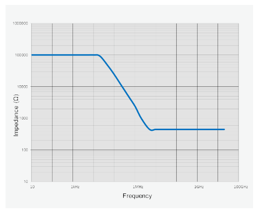
At low frequencies (DC-100Hz), the impedance of typical probes looks like a large resistor. Probe impedance specifications at low frequencies range from 40kΩ to 1MΩ. Performance probes are required to measure signals much higher in frequency than 100Hz. Probes are available today with bandwidths that range from several GHz up to 33 GHz. Since performance probes cover a wide frequency band, it is important to understand how the input impedance of a performance probe changes as the input signal increases in frequency. Figure 2 shows how a performance probe that starts with high input impedance at low frequencies can have its input impedance decrease as the input signal’s frequency increases.
Why? The physical structure of the probe and probe tips that form the probe’s attenuation circuit change their impedance as the input signal’s frequency increases. The attenuation circuit extends the dynamic range of the probe’s input amplifier (Figure 3). This attenuation circuit consists of a set of resistors with an attenuation ratio such as 5:1 or 10:1. The attenuator circuit also has a certain amount of parasitic capacitance (Cpar) in the input signal’s path. The parasitics can be caused by several different items. Wire pairs, IC pads, ESD protection circuits and the base of input transistors can all be sources of parasitic capacitance.
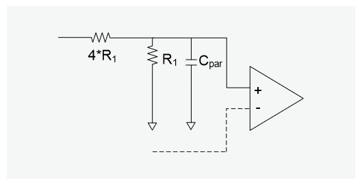
The combination of resistance and capacitance in the attenuator circuit can create a low pass filter that limits the useable bandwidth of the probe. To extend the bandwidth, a set of larger capacitors and resistors are typically added to the input. By matching the component values properly, the bandwidth of the probe can be extended to very high frequencies (Figure 4).
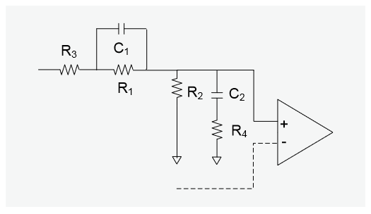
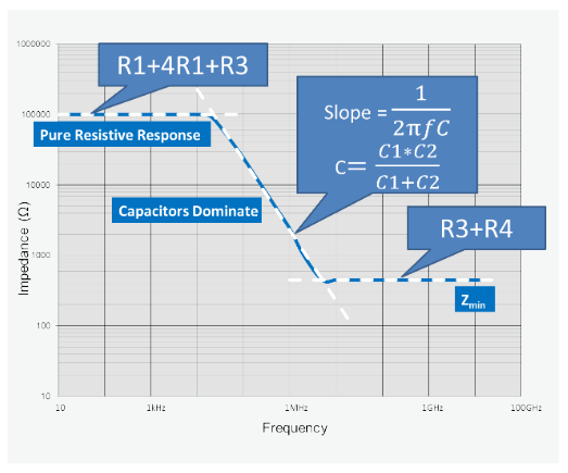
If the input attenuation network is properly designed, the bandwidth of the probe will be very high. However, the impedance of the input will exhibit the decreasing input impedance characteristic that was shown in Figure 2. Looking at that impedance vs. frequency curve again, it is clear that the resistors (R1 and 4*R1) dominate the input impedance at low frequencies. For signals with high frequency components, the capacitors will take over and result in lower impedance as the frequency increases (Figure 5).
The impedance will eventually go to 0Ω if the circuit is purely capacitive. To establish a minimum impedance value for the probe, designers typically include another set of resistors in the attenuation circuit. These resistors, R3 and R4, set a minimum level for the probe’s impedance sometimes referred to as Zmin.
P7700 Chip-on–the-Tip Technology

In the past, probe designers had to make a trade-off between 3 key factors, bandwidth performance, input impedance, and ease of connecting to the device under test. The P7700 series offers an industry-first for high performance probes. These probes use a “Chip-on-theTip” architecture that places the probe’s active input buffer at the end of tip. Modern SiGe processes enable this innovation by providing a set of high impedance, input amplifiers in a very small package. The small probe amplifier package is placed on solder-in tips less than 4 mm from the DUT connection resulting in minimal signal loss, low capacitance, low added noise, and 20 GHz bandwidth. In addition, these active tips are very thin and flexible, making them suitable for probing in very tight spaces. With Chip-on-the-Tip technology, a user doesn’t have to compromise on bandwidth, low loading, or ease of connectivity.
Performance Probe Design Trade-offs and Their Impact
The high frequency design tradeoffs made in the probe's front-end affects its input impedance. Let's consider the actual impact on a device using two high performance probes with different designs. The input impedance of two probes are shown in Figure 6. It is clear that the probe designers made different choices in their probes’ design. One chose a higher capacitance input where the impedance drops to Zmin at relatively low frequencies (probe 1). While the other created a lower capacitance design that maintains its impedance to high frequencies before dropping down to Zmin (probe 2).
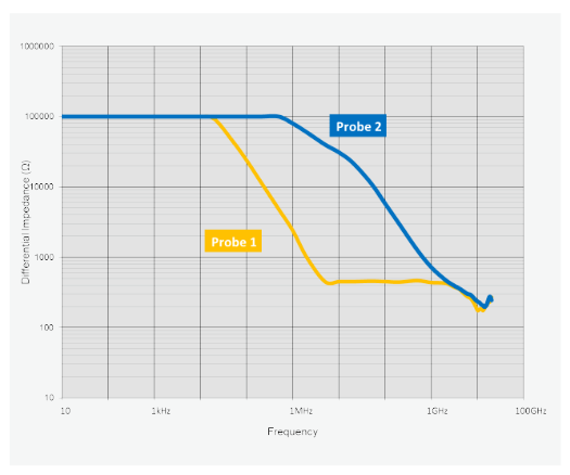
In the past, designing a high impedance input like probe 2 typically meant that the bandwidth of the probe would be limited. While a design like probe 1 achieved high bandwidth at the expense of lower input impedance. That is no longer true as there is now a 20 GHz bandwidth probe with the input impedance of probe 2. See the sidebar: "P7700 Chip-on-theTip Technology" for more details.
PROBING EXAMPLE 1: HIGH SPEED SERIAL
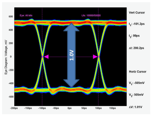
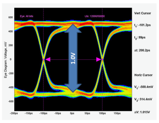
Let’s look at the impact of the different input impedances of these two probes on real signals. Starting with eye diagrams of an 8 Gb/s high speed serial (HSS) link and attaching each of these probes, we’ll study the changes in the signal due to probe loading. This HSS signal has a nominal amplitude of ±500mV. Figure 7 represents the signal in an unloaded state. This picture represents the signal at the transmitter output before any probing is done.
When a probe is attached to this circuit, a portion of the signal’s current is removed by the probe. Figure 8 shows the results for Probe 1 that has a high capacitance input. Since Probe 1 looks like a low impedance at low and high frequencies, the loading on the high speed serial signal is noticeable, but similar across the signal's wide range of frequency components. This loading means that the signal seen by the receiver has been reduced from ±500mV to ±450mV, or 10% lower.
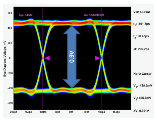
Figure 9 shows how Probe 2, with its high impedance at low and medium frequencies, loads the circuit very little at low to medium frequencies. Compared to the reference eye, the peak amplitude of the topline and baseline of the eye are very similar. The noticeable change in the eye occurs at the higher frequencies, when the signal is changing levels with very fast rising or falling edges.
The loading of this probe at high frequencies creates an eye diagram with an asymmetric look and the rise and fall times of the signal seen by the receiver are slower. While the impedance of these two probes load the HSS signal in different ways, the serial link is likely to continue operating reliably since the eye is still wide open.

PROBING EXAMPLE 2: LOW POWER SERIAL BUS WITH SOURCE IMPEDANCE SWITCHING
In the HSS example, the system’s receiver was able to tolerate a lower signal level and the slowing of the edges. Now let’s consider an example where the device’s source impedance switches levels depending upon the state of the bus. This can be illustrated using a 1 Gb/s MIPI® D-PHY bus signal. In a low power (LP) mode, the D-PHY bus operates in a high impedance state, while in its high speed mode the transmitter and receiver operate as a differential link terminated with 100Ω differential impedance. This switching of the source impedance interacts with the impedance of the probe.
When a probe with high capacitance like probe 1 is connected to the data lines and while they are in the low power mode, the data signals are severely loaded. The loading occurs because when the bus is operating in low-power mode it is in a high impedance state and the frequency range of its signaling is a few MHz. In the 1-10 MHz frequency range, the probe’s impedance is decreasing towards Zmin. Looking at the D-PHY data lines in Figure 10a, notice that the waveform has a rounded top, instead of sharp rising edges and being squared off at the top,. The probe’s capacitance and low impedance slows the rising edge of the pulses.
Using probe 2 with higher impedance and lower capacitance characteristics, results in reduced loading and an improved operation of the D-PHY bus in low power mode (Figure 10b). The higher input impedance and lower capacitance of this probe lowers the loading seen on the D-PHY bus in its LP mode. The high speed mode signals are also accurately represented, because the bus is running as a terminated differential link at that time. The Zmin of probe 2 is higher than the 100Ω differential impedance and the probe loading is unnoticeable.
For the D-PHY bus, probes with input impedance characteristics like the probe 2 are required.

Simulating Probe Loading
Although the improvement in the capability of circuit board layout tools has helped to decrease the risk that high performance digital boards will fail due to signal integrity problems, simulation tools are only as good as the models themselves.
Today’s high performance probes typically come with a model of the probe’s frequency response and its impedance vs. frequency. Using this information, it is possible to simulate the impact of the probe’s load on the circuit.2 The probe used here, as an example, will be a Tektronix P7720 TriMode™ probe. The P7720 probe and its accessory tips are calibrated using a vector network analyzer (VNA) and have the resulting s-parameter description of their responses stored in on-board memory.
The S-parameter models designed into the P7720 TriMode probes provide probe load and response information. Probe load modeling information was extracted from VNA measurements on a custom test fixture. Using this information an equivalent AC circuit for the probe can be constructed to simulate its loading on a circuit (Figure 11).

Tektronix probe models may be used with simulation tools that take SPICE or Touchstone format files as an input. Let’s consider a stimulus that is a 10Gb/s, 211-1 PRBS signal. In the simulator, a 100fF capacitor and VCVS are used to smooth out the input eye to make it more realistic. Figure 12 shows the example circuit simulation and resulting signal using Tektronix iConnect software.


Figure 13 shows the result of inserting the P7720 and solder-in tip circuit model shown in Figure 11 to the example circuit model. Notice the similarity of this eye diagram to the measured eye in Figure 9. This eye diagram shows the loaded signal at the system’s receiver.
Tektronix oscilloscopes perform automatic probe deembedding based upon the probe’s s-parameter data. Using the probe and accessory tip’s s-parameters, the scope software removes much of a probe’s loading effects to more closely resemble the signal in its "unloaded" state.

Challenges When Attaching the Probe to Your Device
Making a connection to a device often requires using wire and solder. The size of the available test points often requires a very small diameter of wire be used for the connection. With modern component and PCB feature sizes shrinking the wire used for connections can be as small as 4 mil (0.1mm) in diameter (Figure 14).

When multiple connections need to be made in a small area, it often requires that the probe tips be spaced apart at different angles with wires that need to reach far from the end of the probe tip. Some probe tips come with leads attached to them that can be used for this purpose, but even these leads can come up short. Especially when 3-4 probe tips need to be attached in the small area (Figure 15).

To maximize probe performance and signal fidelity, Tektronix recommends keeping the wire length for signal and ground connections as short as possible. This recommendation is based upon the fact that adding wires to the tip of a probe adds undesirable parasitics in the form of capacitance and inductance. However, some connections require using longer wires to connect the probe tip to the DUT. Wondering how much parasitic elements are added and how long the wire length can be before a probe’s bandwidth is severely reduced?
Although there are too many variables to know exactly how the bandwidth of the probe will be reduced by a particular wire length, Tektronix has collected data on many probe types with solder-in tips using various lengths of wire. Data from these experiments are published in the probe manuals as examples of probe responses with progressively longer wires.
Figure 16 shows the response of a P7720 TriMode probe with a P77STFLXA solder-in tip with the wire leads cut to various lengths. The step generator that was used as a signal source for these screenshots has a 23ps 10-90% rise time. The caption under each figure contains data for rise time measurements (10%-90%) and the equivalent bandwidth. These screenshots can be used as a rough guide to gauge the effects of wire length, but actual results may vary depending on the other factors like characteristics of the device under test (for example, rise time and source impedance) and the precision of the solder connection.
For wire lengths longer than 0.12 inches, the bandwidth of the P7720 probe is lower that its 20 GHz specification. Connecting to hard to reach test points may require using longer wire lengths. Making a trade-off of lower bandwidth for easier connections may be acceptable if the bandwidth required to measure a signal is less than 20 GHz. Check the manuals for your specific probe to obtain additional rise time and wire length information.


Capturing Single-ended and Differential Signals
Modern performance probes offer the flexibility to connect to a circuit and measure a signal differentially; in a single-ended, ground referenced manner; and in a mode where the circuit’s common mode voltage level is measured. The Tektronix P7500, P7600, and P7700 probe series offer this TriMode functionality (Figure 17).

GROUND OR NO GROUND?
TriMode probes can acquire a differential signal with only the probe’s A and B inputs connected to the DUT. Why would a ground connection be needed or useful in this scenario? Only connecting the differential inputs of the probe may be most convenient due to space limitations near the probe tip and usually provides good electrical performance. However, if there is space for another connection and a circuit ground near the probe tip, hooking up a ground connection is recommended, because it may help avoid a situation where a large potential on the DUT’s ground causes the test signal to drift outside of the linear range of the probe’s input amplifier. Ideally, it is a good idea to hook up the differential inputs and the ground too in order to avoid clipping of the signal in the probe amp.
SINGLE-ENDED – WHAT INPUTS SHOULD BE USED?
When acquiring single-ended, ground referenced signals, the user has two choices. First, the probe’s A or B inputs can be connected to the signal and one of the probe’s ground connections can be connected to ground. An advantage of this connection method is that it is possible to connect the probe to two single-ended signals at the same time. By connecting two single-ended signals to the probe at once, it is easy to switch between viewing the signal on the A input and the signal on the B input simply using the switch matrix built into the TriMode probe.
If only one single ended signal will be connected to the probe, the user has the choice of connecting the A input to the signal and the B input to ground or connecting the A input to the signal and the probe’s ground input to the DUT’s ground. In this situation, Tektronix recommends using A-B mode with the B input connected to ground. The reasons for this recommendation include the fact that with the B input left unconnected, there is a possibility of an interfering signal coupling into the probe’s input and distorting the measured signal acquired on the A side.
A second reason for using A-B vs. A-ground is that it is often more convenient to connect the probe’s differential inputs to a device and keep the wire lengths short. The probe’s ground connections are set back from the tip and may not be as convenient to connect to a DUT with tightly spaced test points.
Conclusion
This application note has discussed many of the challenges experienced when probing high performance circuits. Details of probe loading were discussed and explained so loading that impacts the operation of the DUT can be avoided. Other aspects of probing such as signal access using thin wires and how best to utilize TriMode probes were explained. Signal fidelity issues and impact on the DUT can often be avoided with careful attention to the probing methods.