联系我们
与泰克代表实时聊天。 工作时间:上午 9:00 - 下午 5:00(太平洋标准时间)。
致电我们
工作时间:上午9:00-下午5:00(太平洋标准时间)
下载
下载手册、产品技术资料、软件等:
反馈
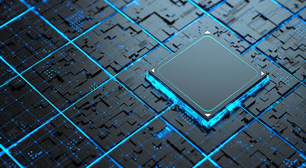
准确、可重复的 PCIe 测量
近二十年来,PCI Express® 技术已成为广泛采用的高速串行接口连接标准。最新的 PCIe® 规范满足了数据密集型市场的需求,例如人工智能/机器学习和高性能计算。
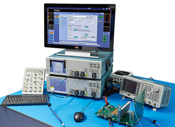
我们的 PCIe 自动化测试解决方案能够处理设置和校准,显著降低了测试复杂性。与低噪音测量硬件相结合,可实现快速、准确且可重复的信号完整性测量。作为 PCI-SIG® 工作组的活跃投票成员,我们拥有发射机、接收机、参考时钟和锁相环 (PLL) 验证所需的丰富专业知识。
PCI Express、PCIE 和 PCI-SIG 是 PCI-SIG 的注册商标和/或服务商标。
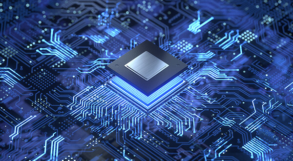
面向 PCIe 的全面自动化测试解决方案
业界领先的 PCIe 6.0 Base 和 CEM 发射机和接收机测试解决方案
PCIe® 6.0 是一种多功能的高速串行接口标准,用于连接现代计算系统中的各种组件。它采用 PAM4 信令和前向纠错 (FEC),实现了突破性的 64.0 GT/s 数据传输速率,可为要求苛刻的应用带来更快的处理速度和更流畅的性能。
泰克的直观工具针对信噪失真比 (SNDR) 和不相关抖动等数据测量以及最新规范所强制要求的接收机压力眼图 TP3/TP2 校准和仪器噪声补偿提供超乎寻常的支持。
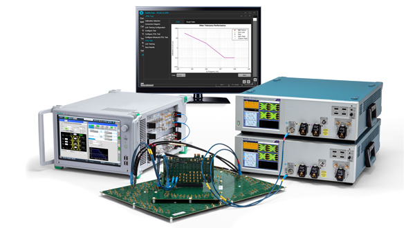
与前几代产品一样,PCIe 6.0 验证和一致性测试对于确保符合 PCI-SIG 为 BASE 和 CEM 制定的标准至关重要。借助泰克的 PCIe 6.0 发射机 (Tx) 测试解决方案,工程师可以解决最新出现的设计和验证问题。对于 PCIe 6.0 接收机 (Rx) 测试解决方案,泰克和安立公司合作,通过将泰克的 DPO70000SX 实时示波器与安立公司的 MP1900A 误码率测试仪 (BERT) 配对,提供了卓越的 Rx 测试解决方案,两者均由泰克开发和支持的测试自动化和分析工具控制。
联系我们,了解您的 PCIe 6.0 测试应用程序。
PCIe 发射机测试解决方案
通过提供自 2.5 GT/s 至 64.0 GT/s 的 PCIe 发射机验证和一致性解决方案(第 1 代至第 6 代),我们的 PCIe 发射机测试解决方案支持向后兼容。从早期的芯片级的电压/时序表征到平台级的发射机和参考时钟测量都在支持的范围内。泰克技术领导者通过包含所有工程变更通知 (ECN) 并支持 PCI-SIG 一致性研讨会作为获得认可的解决方案,从而确保这些解决方案保持紧密相关。
PCIe 接收机和 PLL 测试解决方案
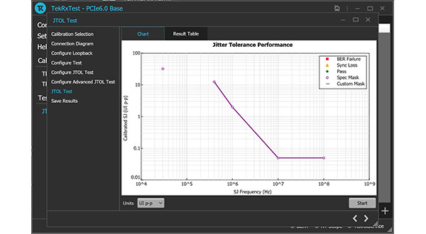
由于在高损耗通道下校准压力眼图信号的灵敏度原因, PCIe 接收机验证非常困难。通过泰克的 PCIe 接收机测试解决方案,您可以充满信心地让设计以必要的误码率 (BER) 目标值全面通过测试。我们直观的分步骤工具为 Anritsu MP1900A BERT 提供了链路训练例程,以确保准确测试您的接收机。自动化测试支持压力眼图校准、最新的发射机和接收机链路均衡一致性测试、自定义 BER 运行以及抖动容限检定。此框架还支持轻松地测量发射机 PLL 带宽和峰值。
Compute Express Link (CXL)
数据中心架构必须能够不断地响应数据移动和访问的需求,同时最大限度降低功耗,提高效率,并支持更大规模和更为多样的应用。利用 PCIe 物理层的优势,CXL 可满足这些要求,允许处理器高效访问相同的内存资源,一起通信,并在单个架构上运行。泰克提供的物理层解决方案支持最快的 CXL 数据速率 (32 GT/s) 以及此新兴技术可能带来的各种各样的外形。