联系我们
与泰克代表实时聊天。 工作时间:上午 9:00 - 下午 5:00(太平洋标准时间)。
致电我们
工作时间:上午9:00-下午5:00(太平洋标准时间)
下载
下载手册、产品技术资料、软件等:
反馈
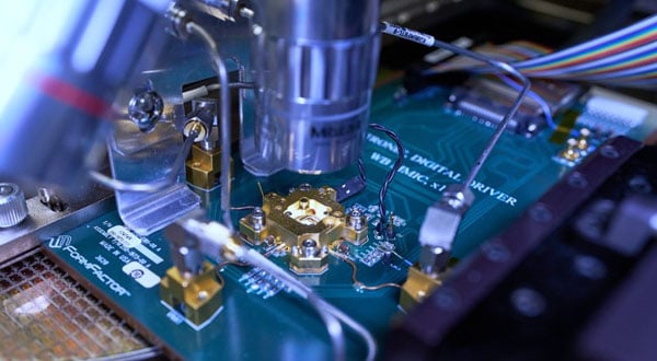
Comprehensive Wafer Test Development and Testing Services
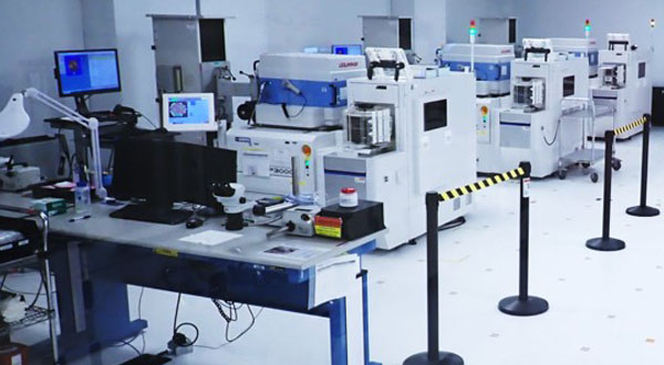
At Tektronix Component Solutions, we provide comprehensive wafer test development and testing services designed to meet the most demanding semiconductor applications. Our state-of-the-art facilities span over 45,000 sq. ft., featuring Class 10,000 (ISO 7) and Class 1000 (ISO 6) clean rooms that ensure optimal conditions for wafer processing.
We specialize in testing a wide range of wafer sizes, including 4", 6", 8", and 12" (100mm, 150mm, 200mm, 300mm). Our capabilities encompass analog, digital, and mixed-signal testing, with advanced test equipment supporting frequencies up to 110 GHz. We offer precise wafer test temperature ranges from -40°C to 200°C, ensuring accuracy and repeatability in diverse environments. Our services feature a wide range of probing technologies and support for both vertical and membrane-style probe cards, making us a trusted partner for all your wafer testing needs.
Our Wafer Testing Process
Project Kick-off & Planning
We collaborate with customers to review requirements, define the testing framework, and select the best testing platforms, probing technologies, and test vectors to meet project objectives.
Development Cycle
Our team develops hardware and software in parallel to meet complex testing needs. Hardware efforts focus on custom probe test boards, collaboration with probe head vendors, and addressing application-specific challenges. On the software side, we create tailored test scripts, ensure full coverage, and integrate with the CSO custom database. Rigorous design review cycles ensure quality and alignment across disciplines.
System Integration & Debug
We integrate the test system with hardware such as probe cards, RF equipment, and ATE systems, followed by rigorous debugging to ensure smooth operation. Initial power-up confirms the functionality of the device, hardware, and software.
Characterization & Finalization
Refined hardware and software enable precise test methodologies for effective experimentation during characterization and limit-setting. Our team specializes in first turn-on of new devices, leveraging expert resources to troubleshoot, debug, and collaborate with design engineers to resolve challenges.
Validation & Readiness
We conduct statistical analyses, including GR&R studies, to ensure consistent, reliable results. Production readiness tasks are completed, reviewed internally, and presented to the customer for final approval.
Our Competitive Edge
Turn-Key Solutions for Wafer Value Stream
For projects requiring wafer processing (e.g., wafer bumping, thinning, dicing), we maintain relationships with various domestic and international industry suppliers and offer supply chain management capabilities to enable a turnkey solution for your microelectronic parts.
- Wafer Fabrication
- Wafer Bumping
- Secure Storage
- Wafer Probing
- Wafer Inspection
- Die Preparation Services
Best in Class Wafer Test Services
Beyond standard development and testing, we offer a wide range of automated wafer test processes that greatly improve accuracy and repeatability, including:
- Automated wafer handling
- Automated probe card changing
- Automated optical probe tip inspection
- Automated optical probe mark inspection
- Automated probe tip cleaning
Customized Wafer Probing
Tektronix employs a team of electrical and mechanical design engineers that can develop customized wafer probe cards and test solutions to meet the most demanding requirements.
For projects requiring wafer processing (e.g., wafer bumping, thinning, dicing), we maintain relationships with a variety of domestic and international industry suppliers and offer supply chain management capabilities to enable a turnkey solution for your microelectronic parts.
Tektronix employs a team of electrical and mechanical design engineers who can develop customized wafer probe cards and test solutions to meet the most demanding requirements.
Understanding Wafer Testing
Ensuring Quality in Semiconductor Manufacturing
Wafer Test (also referred to as Wafer Probe) is a vital step in the Semiconductor Value Stream, focusing on electrical screening and consumption of Known Good Die (KGD). It involves probing individual semiconductor devices on a wafer to identify defects and confirm functionality before further manufacturing.
What Does Wafer Testing Entail?
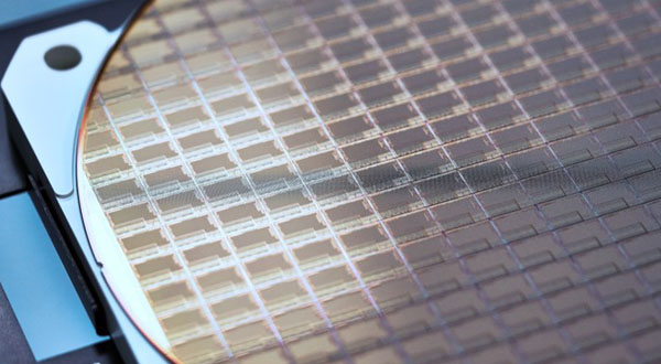
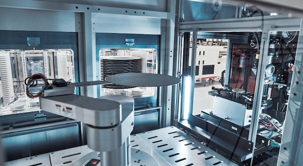
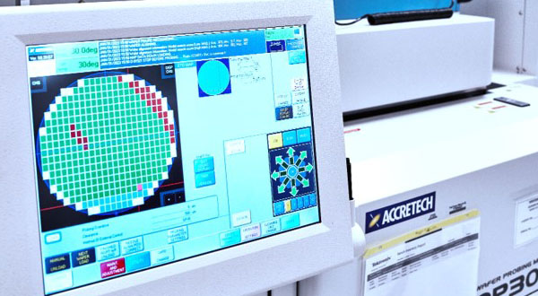
First, let’s start with understanding the form factor of a modern wafer. A wafer is essentially a disc that is no greater than 3/4 mm thick and up to 300 mm in diameter. To put this into perspective, imagine a silicon disc that is half the thickness of a dime and a foot in diameter. Due to the form factor and fragile nature of the wafer, it is impractical to process a wafer by hand (especially since most wafers are bumped). Therefore, in today’s semiconductor testing environment, fully automated equipment is utilized to enable the process. The automation includes both a wafer prober to handle the wafers, a programmed test solution to perform the electrical testing, and robotic equipment to perform inspection and sort wafers.
To connect to the Device Under Test (DUT), a probe head and card must be designed (typically unique to each Integrated Circuit - IC) and integrated with the test station and wafer prober to form the test solution.
A cassette of wafers (up to 25 at a time) is loaded onto the prober, and the screening process begins. An individual wafer is selected, placed on a stage, and manipulated so that each device on the wafer can be accessed and electrically tested. The data for each IC is collected, and a digital map is generated identifying the location and Pass/Fail status. Once complete, the wafer(s) can be sent to the dicing process so that the KGD are ready to be consumed at the next level.
What Are the Benefits of Wafer Testing?
In the era of System on a Chip (SOC) and Heterogeneous Solutions, where integrating multiple complex ICs per package is the norm, the significance of KGD entering the packaging stage cannot be overstated. Wafer Test plays a crucial role in defect detection, ensuring that non-conforming components are identified and prevented from reaching the next stage of production. Paired with continuous Process Monitoring, it empowers engineers to address issues at an early stage, significantly contributing to yield improvement and reduced production costs by eliminating defects in the early steps of the Semiconductor Value Stream.
Wafer Probe FAQs
What are the common testing frequency ranges?
What are the common testing temperature ranges?
The test solutions are designed to accommodate common temperature ranges of -40°C, +100°C, and +125°C, with room temperature support (25°C to 40°C). Specifically, the TEL P8XL model prober can achieve temperatures as low as -55°C, while the Accretech model is capable of reaching down to -40°C.
What are some challenges wafer testing faces today?
Wafer testing is a complex service that faces several key challenges:
- Heterogeneous Solutions: The prevalence of heterogeneous solutions, where multiple devices are integrated into a single package, complicates tracking and management throughout the testing process. This necessitates robust part identification and traceability systems to maintain the integrity of each component.
- Increased Interconnect Density: The shift towards 2.5D solutions has significantly increased interconnect density for a given Integrated Circuit (IC). For example, interconnect spacing on an IC could shrink from 0.150 mm to 0.030 mm, resulting in a 5X decrease on both the X- and Y-axes and an increase in interconnect density of up to 25X. This necessitates the development and qualification of new probing solutions and methods.
- Eliminating Manual Handling: As the demand for IC solutions expands, so does the pressure on wafer testing. To eliminate defects caused by handling, reducing manual intervention is paramount.
What are some opportunities for improvement in wafer testing?
To enhance traceability in wafer testing, integrating non-volatile memory directly into the IC design (instead of relying on laser-scribed human-readable unique identifiers) allows for accuracy and ease of tracking. This integration facilitates capturing wafer lot, wafer number, and row/column information for each IC, contributing to improved part genealogy and tracking throughout the manufacturing process.
As the semiconductor industry evolves to incorporate 2.5D solutions, the increased interconnect density on ICs presents new challenges. Addressing this requires innovative probing solutions and increased collaboration between test providers, wafer test equipment vendors, and probe solution suppliers.
The demand for comprehensive automation in wafer testing is critical for improvement. Automation systems that efficiently eliminate human handling steps can reduce unwanted defects and enhance overall efficiency in the testing environment. By integrating AI and Machine Learning into the inspection process, screening can be optimized to improve effectiveness and address challenges associated with human-dependent procedures.
What is the future of wafer testing?
As demand rises, significant opportunities for innovation arise in overcoming challenges such as heterogeneous integration and increased interconnect density. By integrating non-volatile memory, collaborating on probing solutions, and advancing automation, the future of wafer testing looks promising. As an organization that differentiates itself by providing best-in-class test services, we are excited to be part of this pivotal time in the Semiconductor Value Stream.
What are some common wafer probe applications?
Wafer probing is commonly utilized in the semiconductor industry for various applications, including process control, device characterization, failure analysis, and reliability testing.
What are some types of wafer probes?
There are several types of wafer probes, including manual probes, semi-automatic probes, and fully automatic probes. Manual probes require an operator to manually move the wafer to each test site, while semi-automatic and fully automatic probes can automatically move the wafer to each test site.
What are some factors to consider when selecting a wafer probe?
When selecting a wafer probe, it’s essential to consider factors such as probe tip size and shape, probe tip material, probe planarity, and probe placement accuracy. Additional considerations include the number of probes, the size of the wafer, and the required throughput.