
联系我们
与泰克代表实时聊天。 工作时间:上午 9:00 - 下午 5:00(太平洋标准时间)。
电话
致电我们
工作时间:上午9:00-下午5:00(太平洋标准时间)
下载
下载手册、产品技术资料、软件等:
反馈
Features & Benefits
All Modules
- Up to 70 GHz Bandwidth and 5 ps Measured Rise Time (10 - 90%)
- Lowest Noise for Analysis – 450 μVRMS at 60 GHz, 300 μVRMS at 30 GHz
- Remote Samplers*1 Enable Location of Sampler Near DUT and Ensure Best Signal Fidelity
- Independent Sampler Deskew Ensures Easy Fixture and Probe De-embedding
- Precision Microwave Connectors (3.5 mm, 2.92 mm, 2.4 mm and 1.85 mm)
- Probe Support
TDR Modules
- 15 ps Reflected True Differential Fully Integrated TDR Rise Time (12 ps Incident) and Feature Resolution Below 1 mm
- Efficient, Accurate, Easy to use, and Cost Effective S-parameters up to 50 GHz
Applications
- Impedance Characterization and S-parameter Measurements for Serial Data Applications
- Advanced Jitter, Noise and BER Analysis
- Channel and Eye Diagram Simulation and Measurement-based Spice Modeling
80E02
- Device Characterization, Transmission Quality, Waveform Parameters
- Low Signal Measurements
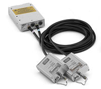
Sampling Modules: 80E02
The 80E02 is a dual-channel, 20 GHz sampling modules and provides an acquisition rise time of 28. Optional 2 meter extender cable is available.
When used with Tektronix 80SJNB Jitter, Noise, & BER software, these modules enable separation of both jitter and noise into their components, understand precise causes of eye closure, and obtain highly accurate extrapolation of BER and 3-D eye contour. When used with 82A04 phase reference module, timebase accuracy can be improved down to 200 fsRMS jitter, which together with the 300 μV noise floor and 14 bits of resolution ensures the highest signal fidelity for the measured signals.
Characteristics
|
|
Application Type |
Channels |
Input Impedance |
Channel Input Connector |
Bandwidth*1 |
|---|---|---|---|---|---|
|
80E02 |
Low-level signals |
2 |
50 ±0.5 Ω |
3.5 mm female |
12.5 GHz*1 |
*1 Calculated from 0.35 bandwidth rise time product
|
|
Rise Time (10% to 90%) |
Dynamic Range |
Offset Range |
Maximum Operating Voltage |
Maximum Non-Destruct Voltage, DC+ACP-P |
Vertical Number of Digitized Bits |
|---|---|---|---|---|---|---|
|
80E02 |
≤28 ps |
1.0 Vp-p |
±1.6 V |
±1.6 V |
3.0 V |
14 bits full scale |
|
|
Vertical Sensitivity Range |
DC Vertical Voltage Accuracy, single point, within ±2 °C of compensated temperature |
Typical Step Response Aberrations*2 |
RMS Noise*2 |
|
|---|---|---|---|---|---|
|
(before step transition) |
(following step transition) |
||||
|
80E02 |
10 mV to 1.0 V full scale |
± [2 mV + 0.007 (Offset) + 0.02 (Vertical Value - Offset)] |
±3% or less over the zone 10 ns to 20 ps; |
+10%, –5% or less for the first 300 ps; ±3% or less over the zone 300 ps to 5 ns; ±1% or less over the zone 5 ns to 100 ns; ±0.5% after 100 ns |
1.8 mV, ≤2.3 mV (maximum) |
*2 Values shown are warranted unless printed in an italic typeface which represents a non-warranted characteristic value that the instrument will typically perform to
Physical Characteristics
|
|
Dimensions (mm/in.) |
Weight (kg/lbs.) |
||
|---|---|---|---|---|
|
|
Width |
Height |
Depth |
Net |
|
80E02 |
79/3.1 |
25/1.0 |
135/5.3 |
0.4/0.87 |
-

Product(s) are manufactured in ISO registered facilities. Product(s) complies with IEEE Standard 488.1-1987, RS-232-C, and with Tektronix Standard Codes and Formats. 85W-22189-0

