简介
功率 MOSFET 用途广泛,可用作高速开关。器件的开关速度受内部电容的影响,内部电容在数据表中通常以 Ciss 和 Coss 表示,它们是由输入栅极和漏极电容 Cgs 和 Cgd 得出。除了指定电容外,栅极电荷(Qgs 和 Qgd)也可用于评估 MOSFET 的开关性能。
JEDEC JESD24-2 标准“栅极电荷测试方法”中介绍了测量 MOSFET 栅极电荷的一种方法。在这种方法中,在测量栅源电压与时间的函数关系时,会强制施加栅极电流。根据由此产生的栅极电压波形,可以得出栅源电荷 (Qgs)、栅漏电荷 (Qgd) 和栅极电荷 (Qg)。
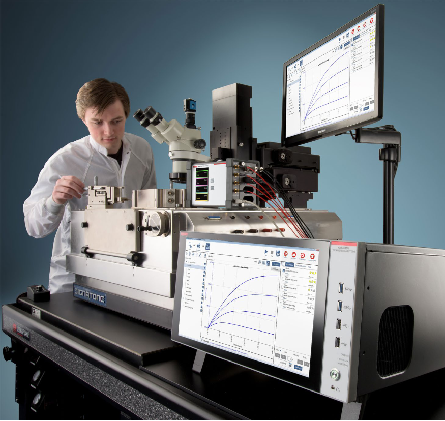
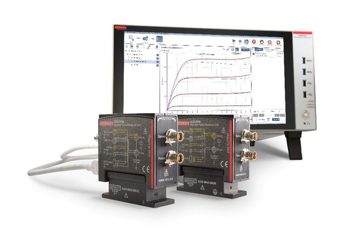
4200A-SCS 参数分析仪支持使用两台“源测量单元”(SMU) 仪器和系统附带的栅极电荷测量测试功能进行 MOSFET 栅极电荷测量。该测试是 4200A-SCS Clarius+ 软件套件提供的广泛测试库中的众多测试之一。本应用指南介绍如何使用 4200A-SCS 参数分析仪根据 JEDEC 栅极电荷测试方法测量 MOSFET 栅极电荷。
MOSFET 栅极电荷测量概述
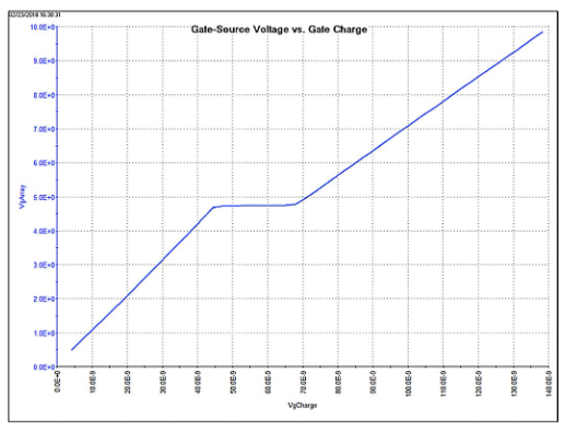
在栅极电荷法中,向 MOS 晶体管的栅极强制施加固定的测试电流 (Ig),并根据流入栅极的电荷绘制测得的栅源电压 (Vgs)。对漏端子应用固定偏压。图 1 显示了功率 MOSFET 的栅极电压与栅极电荷的关系。
栅极电荷 (Q) 由强制栅极电流和时间 (Igdt) 得出。如图 1 所示,栅源电荷 (Qgs) 是达到电压 (Vgs) 几乎恒定的坪区起点所需的电荷。根据 JEDEC 标准,坪(或 Miller)电压 (Vpl) 被定义为 dVgs/dt 最小时的栅源电压。电压坪是晶体管从关断状态切换到导通状态的区域。完成这种切换所需的栅极电荷 — 器件从坪区的起点切换到终点所需的电荷 — 被定义为栅漏电荷 (Qgd),也称为 Miller 电荷。栅极电荷 (Qg) 是指从原点到栅源电压 (Vgs) 等于指定最大值 (VgsMax) 的点之间的电荷。
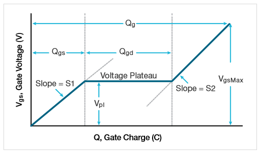
S1 是从原点到第一个坪点的线段斜率。S2 是指从最后一个坪点到指定最大栅极电压 (VgsMax) 的线段斜率。根据 JESD24-2 标准的规定,斜率用于计算 Qgs 和 Qgd。
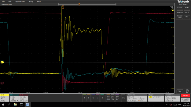
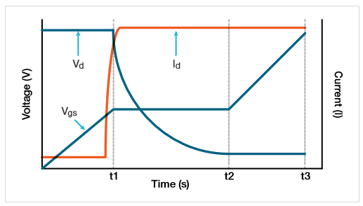
图 2 显示了典型的栅极和漏极波形与时间的函数关系。随着电流被强制施加到栅极,Vgs 会增加,直至达到阈值电压。此时,漏极电流 (Id) 开始流动。当 Cgs 在时间 t1 充电时,Id 保持不变,漏极电压 (Vd) 下降。Vgs 保持不变,直到达到坪的末端。Cgd 在时间 t2 充电完毕后,栅源电压 (Vgs) 再次开始增加,直到达到规定的最大栅极电压 (VgsMax)。
使用 4200A-SCS 进行 MOSFET 栅极电荷测量
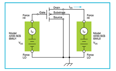
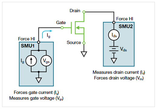
4200A-SCS 使用两台 SMU 仪器测量功率 MOSFET 的栅极电荷。图 3 显示了栅极电荷测试的基本电路图。一个 SMU (SMU1) 的 Force HI 端子连接到 MOSFET 的栅极端子,强制施加栅极电流 (Ig) 并测量栅源电压 (Vgs) 与时间的函数关系。另一个 SMU(SMU2)以指定的限制电流 (Ib) 向漏极施加固定电压 (Vds)。4200-SMU 的最大限制电流为 0.1 A;4210-SMU 的最大限制电流为 1 A。
在栅极电荷测试过程中,栅极电压升高并接通晶体管。在坪区过渡期间,漏极 SMU (SMU2) 从电压控制模式切换到电流控制模式,因为电流超过了规定的限制水平。软件会返回从关断状态过渡到接通状态期间的漏极瞬态电流和漏极电压。
MOSFET 的源极端子连接到 4200A-SCS 机箱的 Force LO 端子或 GNDU。
为 MOSFET 栅极电荷测量配置 Clarius+ 软件
栅极电荷测试位于测试库和项目库中,可通过搜索短语“栅极电荷”在“选择”窗格中找到。在测试库中找到测试后,可通过选择该测试并将其添加到项目树中来添加到项目中。该测试由 GateCharge 用户库中的 gate_charge 用户模块创建。
设置输入参数
在执行测试前,您需要在 Clarius 软件的“配置”窗格中设置输入测试参数(图 4)。输入参数将因器件和使用的 SMU 型号而异。
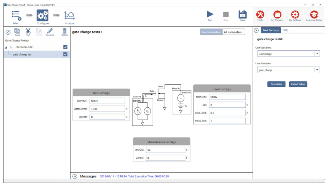
表 1 列出了输入参数的说明。首先,输入与 MOSFET 的栅极 (gateSMU) 和漏极 (drainSMU) 相连的 SMU 编号。源极端子应始终连接至 GNDU 或 Force LO。
gateCurrent (Ig) 参数是 gateSMU 强制施加到栅极的电流大小。漏极电压 (Vds) 是施加到漏极的偏压,drainLimitI 是漏极 SMU 的限制电流。
Coffset 参数用于校正偏移电容,将在以下段落中介绍。
表 1. gate_charge 用户模块的输入参数。
| 输入参数 | 值范围 | 默认值 | 描述 |
| gateSMU | SMU1-SMU9 | SMU1 | 连接到栅极端子的 SMU 编号 |
| drainSMU | SMU1-SMU9 | SMU2 | 连接到漏极端子的 SMU 编号 |
| source | GNDU | GNDU | 源极端子始终连接到 GNDU 上的 Force LO 端子 |
| Vds | ±200 V | 10 V | 漏极 SMU 的偏压大小 |
| drainLimitI | 4200-SMU:0.1A 4210-SMU:1 A |
0.1 A | 漏极 SMU 的限制电流 |
| gateCurrent | ± 1E-5 A | 1e-7 A | 栅极 SMU 的电流大小 |
| VgsMax | ±200 V | 10 V | 栅极 SMU 的最大电压电平。 |
| timeOut | 0 至 300 s | 60 s | 超时前的秒数。 |
| measDrain | 1(是)或 0(否) | 1 | 返回测量的漏极电流 |
| Coffset | 0 或 Ceff | 0 | 在开路情况下运行测试,然后输入返回到数据表的 Ceff 值 |
偏移电容的校正
根据测量系统的布线和连接情况,偏移电容的范围为单个微微法拉到数百微微法拉。这些电容可通过在开路情况下执行 gate_charge 用户模块来校正,获得偏移电容,然后在软件中输入偏移电容值进行补偿。下面介绍如何执行这些步骤:
- 测量偏移电容。设置测试参数,包括输入栅极电流,就像器件连接到 SMU 一样。(增加 VgsMax 只是为了测量 Ceff)。在执行测试之前,提起探针或从测试夹具上取下器件。在开路情况下执行栅极电荷测试。
- 获取偏移电容。执行测试后,将会计算出系统的测量偏移电容,并显示在数据表的 Ceff 列中。Ceff 由最大栅极电压、栅极电流和时间得出。
由于此步骤中测量了开路,因此在执行测试后,数据表中可能会出现 -9 或 -12 的测试状态值。这是因为没有对器件进行测量,所以不存在坪区。但是,Ceff 值是正确的,可以在“配置”视图中作为 Coffset 输入。 - 输入测量的偏移电容并执行测试。在“配置”视图中为 Coffset 输入测量的偏移电容 Ceff。默认情况下,Coffset 为 0 F。在随后的读数中将对偏移电容进行补偿。
执行测试
设置输入参数后,在屏幕顶部选择“运行”即可执行测试。测试运行时,栅极电荷波形将在“分析”视图的图形中实时更新,计算出的输出参数将显示在数据表中。
查看输出参数
测试完成后,将向数据表返回几个参数。表 2 列出了这些参数的说明。
表 2. gate_charge 用户模块的输出参数。
| 输出参数 | 描述 |
| gate_charge | 测试状态值 - 请参见表 3 了解其说明 |
| timeArray | 测量的时间(秒) |
| VgArray | 测量的栅源电压(伏) |
| VgCharge | 测量的栅极电荷(库仑) |
| VdArray | 测量的漏极电压(伏) |
| IdArray | 测量的漏极电流(安) |
| 斜率 | 栅极电压的动态斜率 (dVg/dt) |
| Ceff | 栅极电荷与最大栅极电压之比 |
| Vpl | 坪电压或 Miller 电压(伏) |
| T1 | 坪区域开始的时间戳(秒) |
| T2 | 坪区域结束的时间戳(秒) |
| Qgs | 从原点到第一个拐点或电压坪的栅极电荷(库仑) |
| Qgd | 栅极电荷曲线两个拐点之间的栅极电荷(库仑) |
| Qg | 从原点到 VgsMax 的栅极电荷(库仑) |
绘制结果图
由此产生的栅源电压可以绘制成栅极电荷或漏极电流的函数关系图,漏极电压可以绘制成时间的函数关系图。图 5 是 4200A-SCS 生成的典型栅极电压波形
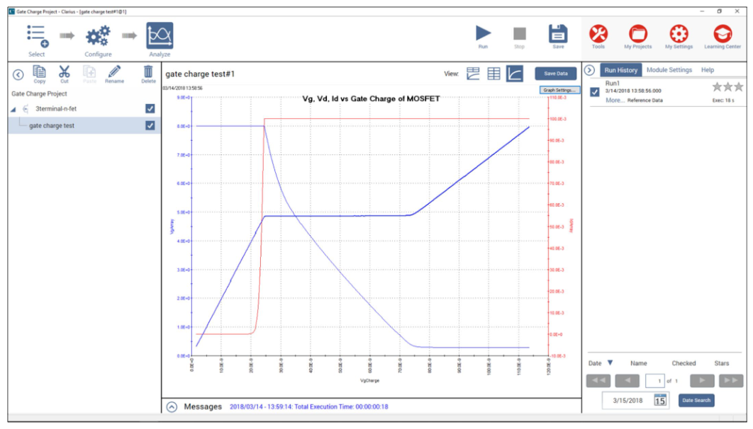
除了绘制 Vgs、Vds 和 Id 之外,还可以绘制 MOSFET 栅极电荷或时间的函数关系图。图 6 显示了 Clarius 软件分析视图中的图形,其中显示了所有三个参数的栅极电荷函数关系图。在这种情况下,电压显示在 Y1 轴上,电流绘制在 Y2 轴上。
检查测试状态
每次执行测试时,都会向数据表中名为”gate_charge“的第一列返回一个测试状态值。表 3 列出了”gate_charge“列中返回的测试状态值及其相应的说明和注释。
表 3. 测试状态值
| 测试状态 | 描述 | 说明 |
| 1 | 无错误 | 测试成功。 |
| -1 | 栅极 SMU 不存在 | 指定正确的 SMU。 |
| -2 | 漏极 SMU 不存在 | 指定正确的 SMU。 |
| -3 | VgsMax > 200 V | 验证栅极电压是否小于 200V。降低栅极电压。 |
| -4 | 漏极电流限值超过 1 A (4210-SMU) 漏极电流限值超过 0.1 A (4200-SMU) |
验证漏极电流是否小于 1 A(或中等功率 SMU 为 0.1A)。降低漏极电流限值 (drainLimitI)。 |
| -5 | 超过功率限值 | 如果 V > 20V,电流应 < 0.1A。降低漏极电流限值 (drainLimitI) 或漏极电压 (Vds)。 |
| -6 | 输入条件错误检查。将 timeOut 限制为 200 s。 | 指定 timeOut < 200 s。 |
| -7 | 测试时间超过指定超时 (timeOut)。 | 增加超时时间。最长为 200 s。尝试增加 gateCurrent,以加快器件充电速度。 |
| -8 | 迭代/测量次数 > 10000。 | 增加栅极电流 (gateCurrent)。 |
| -9 | 迭代/测量次数 < 5 | 降低栅极电流 (gateCurrent)。检查器件和测试设置,检查 SMU 是否正确。 如果在测量开路以进行偏移校正时出现此错误,则可忽略不计。Ceff 值仍然有效。 |
| -10 | 从原点到第一个坪点的点数 < 10 | 减小栅极电流 (gateCurrent) |
| -11 | 计算斜率 S1 出错。相关因子 < 0.9。从原点到第一个坪点的曲线不呈线性。 | 检查器件和测试设置。 |
| -12 | 计算斜率 S2 出错。相关因子 < 0.9。从最后一个坪点到 VgsMax 的曲线不呈线性。 | 检查器件和测试设置。如果 VgCharge 或 VdArray 显示为高电平,请尝试降低栅极电流并重复测试。如果在测量开路以进行偏移校正时出现此错误,则可忽略不计。Ceff 值仍然有效。 |
| -13 | Vds > 200 V | 减小漏极电压。 |
| -14 | gateCurrent > 10 µA | 减小栅极电流 (Ig)。 |
总结
使用吉时利 4200A-SCS 参数分析仪可以轻松测量晶体管的 MOSFET 栅极电荷。通过使用两台 SMU 仪器连接到器件栅极和漏极,Clarius 软件可以轻松获得栅极电荷波形。
要获取更多重要资源,请访问 TEK.COM。