Introduction: What is the Serial Peripheral Interface
In today’s embedded, Internet of Things (IoT) world it seems like everyone has a development board to offer. Boards like those from Arduino and Raspberry Pi are being used to educate a whole new generation of engineers and hobbyists alike. These development boards have processors complete with GPIO, analog inputs, UARTs, timers, and of course I2C and SPI. This document focuses specifically on the Serial Peripheral Interface or SPI bus.
SPI Background
The Serial Peripheral Interface bus (SPI) was originally developed by Motorola in the late 1980s for their 68000 series micro-controllers. Due to the simplicity and popularity of the bus, many other manufacturers have adopted the standard over the years. It is now found in a broad array of components commonly used in embedded system design. SPI is primarily used between micro-controllers and their immediate peripheral devices like memory, sensors, data converters, touchscreens, and displays.
How Serial Peripheral Interface (SPI) Works
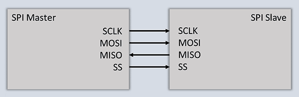
Devices utilizing a SPI connection most commonly communicate via a 4-wire interface. Whenever two devices communicate, one is referred to as the "master" and the other as the “slave”. The master device initiates data transfers, and generates all clock signals. The slave device “reacts” to commands from the master. This reaction may or may not include sending valid data to the master. Because data can be simultaneously transmitted and received, SPI is referred to as a full-duplex protocol.
Figure 1. Master/slave signal lines
As seen in Figure 1, the simple 4-wire version of SPI uses a clock line, two data lines, and a select line. Some manufacturers refer to this as a 3-wire interface; choosing to treat the select line separately from the clock and data lines. Let’s take a closer look at each of these lines.
Serial Clock (SCLK): The Master generates the clock signal to synchronize data transfers between the Master and the Slave(s). This generation of the clock signal by the Master device includes the frequency, polarity and phase.
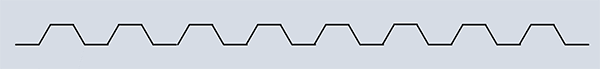
Figure 2. SCLK signal from master to slave
Master Out Slave In (MOSI): The Master generates the signal received by the Slave.
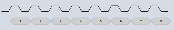
Figure 3. SCLK and MOSI signal
Master In Slave Out (MISO): The Slave generates the signal received by the Master.
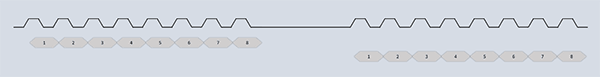
Figure 4. SCLK, MOSI and MISO signal
Slave Select (SS): The Master generates the signal to select individual Slave devices.
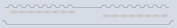
Figure 5. SS signal going from high to low for slave enable
Implementations
Rather than having unique addresses for each device on the bus, SPI uses the SS line to specify from which device data is being transferred. As such, each unique device on the bus needs its own SS signal from the master. There are two types of slave configurations: independent (Figure 6) and cascaded (Figure 7). Most embedded applications will use an independent configuration because of the need to control and interact with specific SPI peripherals. For example, if there are 3 slave devices, there are 3 SS leads from the master, one to each slave as shown in Figure 6.
In Figure 6, each slave only talks to the master. However, SPI can be wired with the slave devices cascaded, each performing an operation in turn, and then sending the results back to the master as shown in Figure 7.
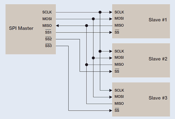
Figure 6. Independent slave configuration
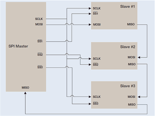
Figure 7. Cascaded slave configuration
As you decide on the configuration of your master and slave devices, it is important to recognize how data will be clocked or transferred through the system. Typically, when a SPI data transfer occurs, an 8-bit data word is shifted out on MOSI while a different 8-bit data word is being shifted in on MISO. If you have multiple slave devices, you may be shifting data from one slave to another before it finally reaches the Master.
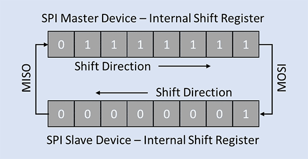
Figure 8. Example of a SPI data transfer
Every Master device should have a pair of registers, clock polarity (CPOL) and clock phase (CPHA), which determine the edges of the clock on which the data is transferred. Each register has two possible states which allows for four possible combinations; all of which are incompatible with one another. As you might expect, this means a master/slave pair must use the same clocking scheme to communicate. If multiple slaves are used that are fixed in different configurations, the master will have to reconfigure itself each time it needs to communicate with a different slave.
SPI is what is known as a “de facto” standard; there is no single, official guide for SPI implementation. As such, you will find a wide variation of implementations. In some cases, the communication from the slave back to the master is not required, and the MISO signal may be left out altogether. In other cases, there is only one master and one slave device with the SS signal is tied to ground. This is commonly referred to as 2-wire SPI. It is even common to find different word sizes and clocking schemes.
Summary of the serial communication protocols (SPI)
Of the serial communication protocols, SPI is: simple to implement (due to simple hardware requirements), capable of fast transfer speeds (with full-duplex communication) and can handle multiple slaves from a single master device. As you look at throughput rates, you should also consider the number of wires required by SPI. With the addition of multiple Slaves, the number of signal paths can become worrisome. Ultimately, the combination of configurations and implementation variations can rapidly become a test and debug challenge if not considered early on in the design process.