
THIS APPLICATION NOTE
- Describes the connection between signal integrity, specifically jitter, and power integrity
- Gives a brief review of jitter measurements and terminology, including eye diagrams and jitter decomposition
- Covers random and periodic jitter on clocks and relates periodic jitter to power integrity
- Describes sources of noise on power integrity, especially noise likely to cause jitter on serial data lines
- Gives an example of the impact of ripple on a power rail causing jitter on a clock
In this application note, we show how to combine jitter and power integrity analysis into a formidable tool for debugging SERDES, circuits, networks, and systems. The application note uses the 6 Series B MSO to demonstrate jitter and power rail measurements. Its low noise contribution makes it well-suited for these measurements. The oscilloscope was equipped with both the Digital Power Management (DPM) option and Advanced Jitter Analysis (DJA). Although the 6 Series B MSO is used as an example, the 5 Series MSO offers the same measurements.
This note focuses on the connections between power integrity and signal integrity. For a detailed look at jitter analysis, please see the Tektronix "Understanding and Characterizing Timing Jitter" Primer (document 55W-16146-6 https://www.tek.com/primer/understanding-and-characterizing-timing-jitter-primer).
Jitter on Serial Data Lines and Power Rail Analysis
Jitter analysis often leads directly to a bug's root cause, but when it doesn't, power rail analysis is the next step. Jitter and power are analyzed in both the time and frequency domains. Comparing PJ (periodic jitter) frequencies in the TIE spectrum to spurs in the power ripple spectrum is a fast and accurate way to identify signal integrity problems caused by the PDN (power distribution network).
Jitter is measured relative to the system clock. Systems that use embedded clocking, where the clock is recovered from data transitions, mitigate low frequency jitter but must be analyzed with a scope capable of emulating the precise clock recovery scheme. The 6 Series B MSO (Mixed Signal Oscilloscope), Figure 1, has both user-programmable clock recovery schemes and many of the clock recovery schemes specified by the standards.

In addition to its jitter and power integrity capabilities, the high bandwidth and low noise of the 6 Series B MSO make it ideal for debugging; 5 Series MSOs offer the same capabilities but with different measurement specifications.
SI & PI Contribute to Errors
Digital errors are caused by jitter and noise. Noise is a broad term for variations in the signal amplitude. Jitter is the variation in the timing of bit transitions with respect to the data-rate clock, the so-called time interval error (TIE). Jitter is caused by both phase noise and amplitude noise-to-jitter conversion. Noise-to-jitter conversion introduces problems from crosstalk, EMI (electromagnetic interference), and random noise.
Signal integrity analysis concentrates on the performance of the transmitter, reference clock, channel, and receiver in terms of the BER (bit error rate). Power integrity focuses on the PDN's ability to provide constant voltage power rails and low impedance return paths. SI and PI have broad interdependence. The PDN can cause noise and jitter. The circuit design and components - chip package, pins, traces, vias, connectors—affect the impedance of the PDN and hence the quality of the power supplied.
Debugging SI Problems Starts with the Eye Diagram
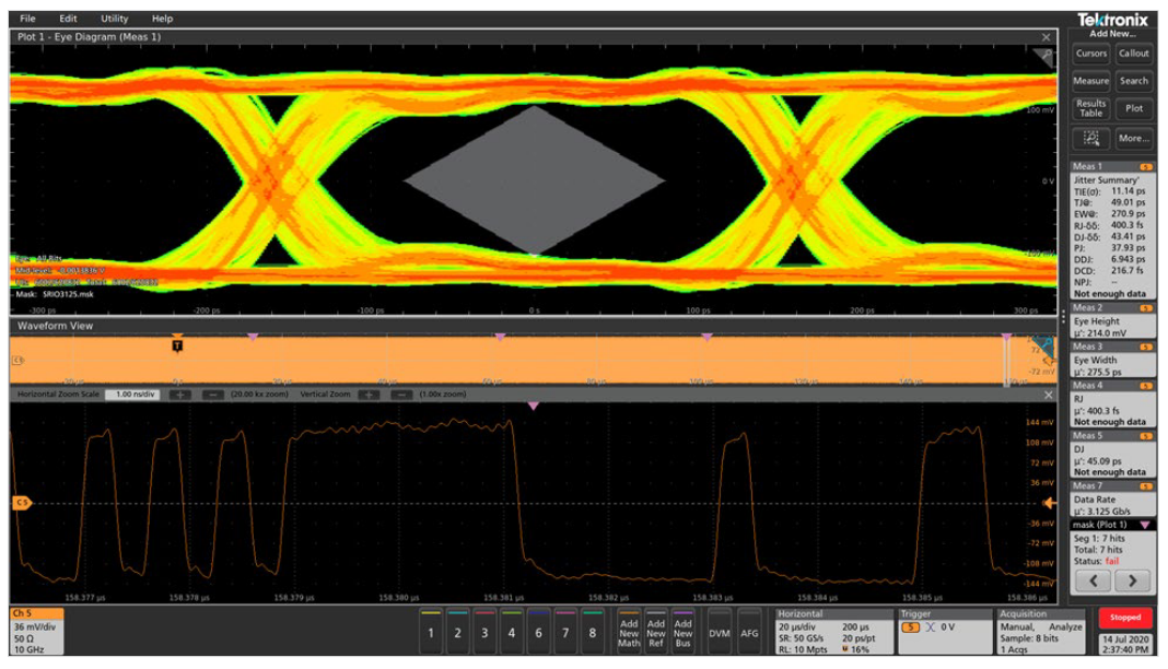
Hardware debugging can start with eye diagram analysis. The eye diagram consists of overlapping waveforms relative to a clock, Figure 2.
The horizontal width of the crossing points indicates jitter and the vertical width of the top and bottom of the eye indicates noise. A wide-open eye should correspond to a low BER. An easy way to gauge signal quality is to perform a mask test.
Some standards specify a mask that enables a simple evaluation of signal integrity on a device under test. On the 6 Series B MSO, masks can be selected from a list of standardsbased masks or custom-built.
Unfortunately, passing a mask test does not guarantee that the system operates below the maximum allowed BER (typically, BER ≤ 1E-12).
JITTER ANALYSIS
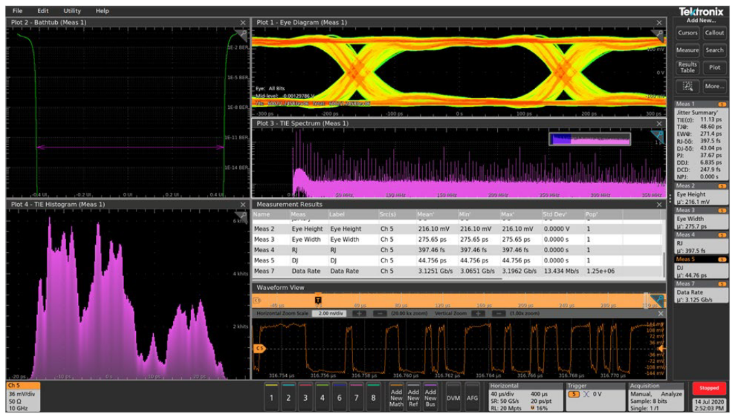
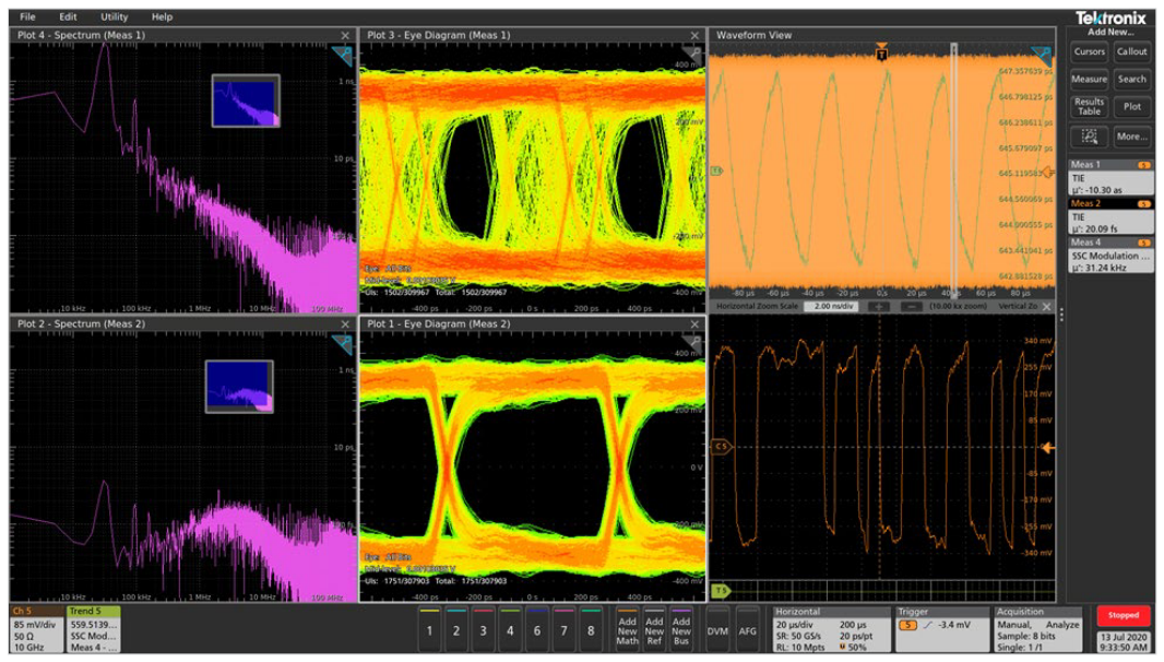
Whether or not we pass the mask test, if the signal integrity is still in question, the next step is to perform jitter analysis. Figure 3 maps the breakdown of jitter into its components and sub-components, and Figure 4 shows a Jitter Summary measurement including the bathtub plot, eye diagram, TIE spectrum and histogram, jitter measurement results, and waveform.

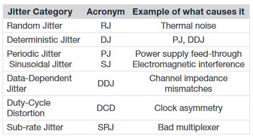
The breakdown of jitter starts with the separation of the TIE distribution into its random and deterministic components, RJ (random jitter) and DJ (deterministic jitter). DJ is further separated into jitter that is correlated to the sequence of bits in the data—DDJ (data-dependent jitter) and jitter that is uncorrelated, such as PJ (periodic jitter).
Widespread crossings on eye diagrams can indicate RJ. Eyes that appear to consist of many nearly distinct lines indicate DDJ, likely from impedance mismatches in the signal path, but eye diagram analysis is of little help in finding the root causes of eye closure. When equipped with the optional Advanced Jitter Analysis (DJA) package, a 6 Series B MSO can measure the types of jitter that can find hardware bugs: TIE, RJ, DJ, DDJ, PJ, TJ (total jitter), EH (eye height), EW (eye width), eye high, and eye low. Table 1 lists different types of jitter and examples of what causes them.
RJ & PJ ON CLOCKS
Clocks set the timing of bit transitions in transmitters and the slicer timing in receivers. Distributed clocks provide a common timing reference for related components and can be observed directly on a scope.
In an embedded clock system, the clock signal cannot be observed directly. The oscillator is integrated in the transmitter chip and the receiver recovers a clock signal from the data. CR (clock recovery) circuits extract data-rate clocks from data transitions using PLLs (phase-locked loops), DLLs (delay-locked loops), or the like. Embedded clocks have a couple of advantages over distributed clocks: first, they don't require extra traces for distribution; and second, they filter low frequency jitter.
Clock noise propagates onto the signal as RJ and/or PJ. If RJ on a data-rate clock is too high, clock phase noise is the likely culprit. While phase noise is inevitable on clocks, the presence of large amounts of observed PJ indicates that something is wrong.
ANALYZING JITTER ON DISTRIBUTED CLOCKS
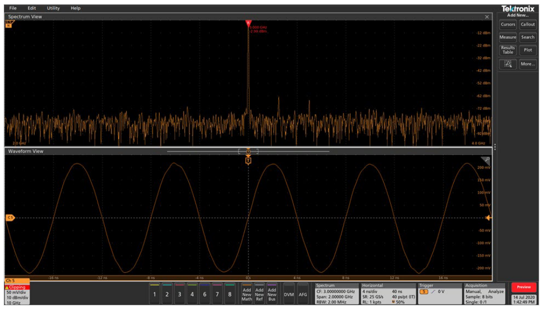
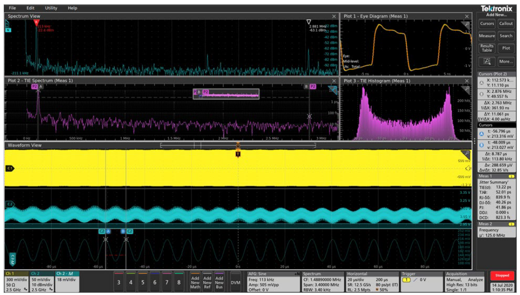
Since the clock is accessible to a scope probe in a distributed clocking system, we can analyze it in the Spectrum View on the 6 Series B MSO. The resonance should be sharp, narrow, and free of harmonic spurs. All resonances have some near-carrier phase noise, the source of RJ, but wide, lumpy resonances with excess white noise are caused by noisy, resistive, or overheated electronics. Spurs cause PJ and can be caused by vibrations and EMI, likely from the PDN, which we'll come back to.
The clock spectrum and waveform shown in Figure 5, has a clean, sharp resonance, though there are a couple of spurs about 50 dB below the resonance whose effects aren't visible in the time domain. Spurs can cause PJ in the data signal, but with the spur frequencies in hand, we can often find the problem by checking the system design for oscillators or switching circuits that could be radiating EMI at those frequencies.
ANALYZING JITTER ON EMBEDDED CLOCKS
In most cases, transmitters and receivers in embedded clocking systems do not provide pin access to the reference or recovered clock, but we can still analyze it.
To separate the clock from other aspects of the system, analyze a repeating test pattern: a fixed number of 0s followed by the same number of 1s, like 01010. The alternating pattern has the advantage of removing the jitter that depends on the bit sequence, DDJ (data-dependent jitter).
Recovering a clock from the data gives the receiver the ability to track low frequency jitter. Jitter at frequencies below the CR bandwidth appears on both the data and the clock that positions the slicer sampling point. When the timing of the slicer has the same jitter amplitudes and phases as the signal, that jitter won't cause errors.
On the other hand, jitter at frequencies above the CR bandwidth can cause errors. The CR bandwidth is specified by the standard, which is often set by a golden PLL (i.e. fd/1667).
To analyze the relevant jitter frequency band, the scope must capture enough time to contain the lowest frequency components of the clock. The 6 Series B MSO emulates clock recovery in software that you can configure yourself or select from a list of PLLs specified by standards.
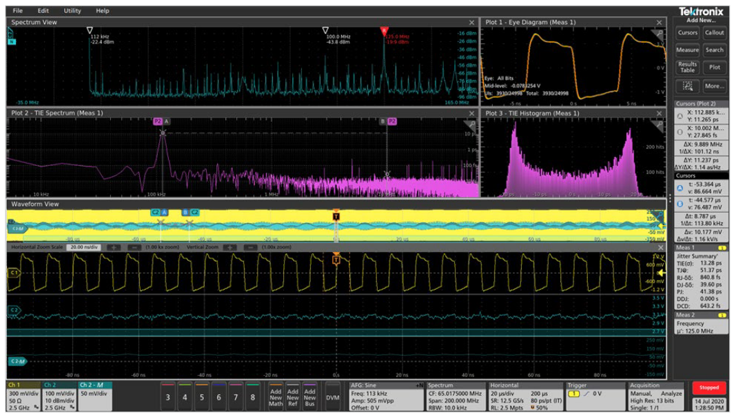
Figure 6 shows the effect of low and different clock recovery schemes; constant clock CR on top, Type II PLL on bottom, and, from left to right, the TIE spectrum, eye diagram, and waveform. PJ shows up as spurs in the spectrum and RJ as the noise floor.
In the top row of Figure 6, the constant clock frequency has much different jitter amplitudes and phases than the data jitter. The result is an eye diagram and waveform with poor signal integrity that results in high BER. On the bottom, the Type II PLL recovered clock has the same low frequency jitter as the data, effectively filtering both RJ and PJ at frequencies within the CR bandwidth. The result is an eye and waveform with good signal integrity and low BER.
Even with the Type II PLL's clock, the spurs in the TIE spectrum show evidence of PJ. Again, comparing with the spur frequencies in hand, we can check the system design for any component that is radiating EMI at those frequencies and find the problem.
Unfortunately, fixing problems with PJ is often more complicated than finding the corresponding oscillator in the circuit. When there is no obvious PJ source, we have to analyze the system's power integrity. Power rail ripple is a common cause of PJ and sometimes RJ, too.
JITTER AND THE POWER DISTRIBUTION NETWORK
The PDN's job is to sustain a constant voltage and sufficient current supply to every active component. It impacts the performance of every element, active or passive. The PDN includes the whole system, not just the VRM (voltage-regulator module) and internal chip power distribution, but every interconnect, trace, via, connector, capacitor, package, pins, and ball-grids. Its performance depends on the SERDES properties and the effective series impedance of the system as a whole; ESR, ESC, and ESL (effective series resistance, capacitance, and inductance).
PJ & GROUND BOUNCE
Power rail noise, often called ripple, is typically a few millivolts. Accurate measurements of mV noise on a power rail at GHz frequencies requires high bandwidth probes with high DC impedance that act as 50 Ω transmission lines at highfrequencies. The TPR1000 and TPR4000 power rail probes are designed explicitly for this purpose. Power analysis can be automated on multiple power rails with the optional 6 Series B MSO Digital Power Management (6-DPM) analysis package which conveniently includes key jitter measurements (TIE, RJ, DJ, PJ).
Switch-mode power supplies regulate the voltage between the power rail and the return path (a.k.a., "ground") by continuously switching between low dissipation on and off states, achieving constant voltage by varying the on/off duty cycle. By avoiding high dissipation states, they waste much less power than linear supplies. Unfortunately, the pattern of on/off pulse-widths that drive the switching elements can induce "switching noise" and cause PJ.
Switching occurs at fixed frequencies that should be recorded on the VRM data sheet. If the ripple spectrum, top left of Figure 7, and the TIE spectrum, just below it, both have spurs at the switching frequencies, then we know the source and can address the design. Notice the large coinciding spur at the red marker in Figure 7. The TIE histogram to the right of the TIE spectrum has the signature sinusoidal jitter distribution (horseshoe), PJ at one frequency
Power supplies can introduce random noise that contributes to RJ. The power rail random noise shows up in Figure 7 as the noise floor of the Spectrum View plot in the upper left. RJ is calculated from the noise floor of the TIE spectrum. In this example, the random noise due to power ripple is very low, and RJ is tiny, about 0.84 ps.
PJ & GROUND BOUNCE
During logic transitions, transmitters and receivers source or sink current from the PDN. When multiple signals switch between levels simultaneously, they can deposit or remove substantial charge from the power rail and/or ground plane. The short-term introduction of charge density alters the voltage of what should be a common ground across the conductor. The resulting voltage variation is called ground bounce or, equivalently, simultaneous switching noise (SSN).
Before continuing, we should clarify a couple of things. First, by "ground" we’re referring to the desired common reference voltage of the return path which is usually defined to be 0 V.Second, "simultaneous" means that the components source or sink charge during the time interval when their rise/fall times overlap.
SSN looks random in the time domain but not in the frequency domain. Data signals are composed of many frequency components—the fundamental or Nyquist frequency and perhaps as many as two higher harmonics, plus the subharmonics from consecutive identical bits. Simultaneous switching can occur at any of these frequencies. Thus, SSN is periodic noise with many low amplitude spurs that can cause PJ.
To confirm that the PJ is caused by SSN, compare the power rail spectrum, top left of Figure 8, with the TIE spectrum, just below it. The high amplitude spur that appears at the same frequency in both spectrums indicates a large PJ contribution from SSN.
Summary
Signal integrity and power integrity are a feedback loop.Every element of the network, every trace, via, connector, pin, package, etc, affects the PDN impedance and the impedance of every channel, and every active component can alter the voltages of power rails and ground planes.
The eye diagram can tell us a lot about signal integrity, but it rarely helps us identify specific problems. Analysis of the TIE distribution breaks jitter into components that provide clues of where problems lie. High RJ usually means a noisy clock, but it can also indicate random noise from the power supply.
PJ can indicate a faulty clock, power supply switching noise, or ground bounce/SSN. Comparing the power rail ripple spectrum to the TIE spectrum can isolate the problem in two steps. Spurs in the TIE spectrum without any corresponding spurs in the power rail spectrum indicate the clock; one or two spurs at the same frequencies in both spectra indicate power supply switching noise; and a large number of spurs common to both spectra indicates SSN. In each of these cases, combining jitter and power analysis isolates otherwise difficult problems.
Signal integrity and power integrity are often considered separate disciplines, but we’ve seen that finding problems associated with high jitter requires understanding both.Fortunately, the 6 Series B MSO has the necessary tools to join the two disciplines in an easy to use touchscreen environment.