The demand for efficient power is accelerating as electrification remains a key driver to reduce carbon emissions. Wide bandgap technologies such as silicon carbide (SiC) and gallium nitride (GaN) are key enablers today to improve power conversion efficiency compared to traditional silicon devices. Engineers must re-evaluate their approaches to validation and testing to meet the challenges of an electrified world.
The demand for efficient power is accelerating as digitization and electrification remain key drivers to improving productivity and environmental responsibility, respectively. Access to data and energy are increasingly being delivered via alternative energy versus fossil fuels, driven by requirements to reduce carbon emission through regional mandates and regulations. This is resulting in both public and private scale investments in new semiconductor technologies and supply chain to accelerate the efficiency of semiconductor power transistors, power modules, power management ICs (PMICs) and power conversion/ inversion systems.
While low power, low-level voltage and current control semiconductor devices and designs have matured, investments are shifting to higher power performance required to improve efficiencies to support the power demands for data center power supplies (digitization) and automotive EV power train, battery management systems and electric motor drivers (electrification). Looking beyond just data center and automotive applications, investments are also focusing in other areas of electrification that offer substantial returns on investment including grid energy storage, larger forms of transportation such as heavy duty vehicles, rail systems and the electrification of aircraft such as the upcoming Urban Air Mobility systems.
Regulatory and economic pressures continue to push the state-of-the-art in industrial and other high-voltage power electronics toward designs that are smaller, faster and more efficient. The power-density advantages of smaller and lighter designs are particularly evident in spaceconstrained and/or mobile usages such as electric vehicles, but compact power electronics are more broadly desirable as well, especially from the standpoint of reduced system cost. At the same time, efficiency is growing in importance as governments introduce financial incentives and more stringent energy-efficiency regulations.
The need to enact greater energy efficiency in power electronics stretches from the point of power generation to the point of consumption. Power converters operate at multiple stages throughout the generation, transmission and consumption chain, and, because none of those operations is 100% efficient, some power loss occurs at each step. Chiefly due to energy lost as heat, these reductions in overall efficiency multiply throughout the cycle.
Likewise, in addition to increasing efficiency, reducing the size and weight of power conversion equipment is critical. Smaller, lighter-weight components typically correspond to lower capital expense (CAPEX), which complements the reductions in operating expense (OPEX) associated with greater efficiency. Efficiency, size and weight of power equipment are critical design aspects for many applications. In the context of an electric vehicle, for example, all three factors contribute to increasing the range of the vehicle between charges, while lower equipment cost helps in the effort to bring overall vehicle cost to parity with that of conventional vehicles.
A critical challenge facing the power electronics industry as it works both to reduce physical size and to increase energy efficiency is that these design goals typically compete with one another. For example, increasing the switching frequency of converter circuits allows the size of components such as inductors, transformers and capacitors to be reduced. That helps enable more compact devices at lower production cost. On the other hand, higher switching frequencies also generate additional heat and the risk of electromagnetic inference (EMI). Accordingly, the power lost through that heat can create product quality and OPEX concerns associated with reduced energy efficiency.
While traditional silicon technology will still be used in power applications where it makes sense, wide bandgap semiconductors including gallium nitride (GaN) and silicon carbide (SiC) are exceeding the capabilities of traditional silicon-based devices. Their adoption is an effort to overcome limitations of silicon that stem from it being a narrow bandgap material, which leads to undesirable conductive leakages that become more pronounced with increases in temperature, voltage or frequency. GaN and SiC typically have much higher power density, smaller size, better high temperature performance, higher frequency response, lower leakage and lower ON resistance than silicon, all of which add up to greater operating efficiency.
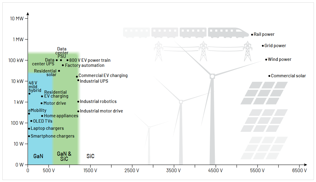
Wide bandgap (WBG) semiconductors are well suited for fast charging of devices through reduction in conduction losses and faster switching speeds. GaN has driven a reduction in size while increasing power density, helping to improve everything from the battery charge time in cell phones, hand power tools and portable personal healthcare monitoring systems, as well as in the growing use cases for electronics power supplies and RF power amplifiers. GaN is also very suited for infotainment and other cockpit applications for electric vehicles (EV).
By contrast, the technologies surrounding SiC are better suited to higher power implementations such as power transmission, large-scale HVAC equipment and industrial systems. Compared to silicon metal-oxide-semiconductor field-effect transistors (MOSFETs), SiC MOSFETS are capable of operating at higher voltages and higher temperatures. Under these conditions, SiC provides higher performance, efficiency, power density and reliability. This combination of benefits is helping designers reduce the size, weight and cost of power converters, making them more competitive especially in lucrative market segments such as aerospace, military and EVs.
Transitioning from traditional silicon to wide bandgap semiconductors results in power module designs that can be physically smaller than what came before, while also increasing MOSFET switching speed and energy efficiency. As competitive pressures make these design parameters more critical, design engineers must reevaluate their approaches to validation and testing. While the types of testing that are required during the design and production of power conversion devices and systems are similar to what was required for previous generations of devices, the adoption of wide bandgap materials requires added rigor in that testing.
Engineers continue to demand higher measurement accuracy and the ability to better understand the demands for higher power densities and efficiency. Demand for functional and reliability testing at the device or subsystem level to ensure designs based on new materials are robust in critical applications outside the consumer space where the reliability of systems over a long timescale is critical to meet the necessary regulation and safety requirements. The drive for energy efficiency in particular is a significant contributor to the need for added rigor in testing, and data measurements must be robust enough to meet regulatory and certification requirements, as well as current JEDEC JC-70 Wide Bandgap Power Electronic Conversion Semiconductor standards.
Tektronix is addressing many of the characterization and validation testing requirements to enable engineers to bring their products to market faster to meet the challenges of electrification. The company is making significant advances in test and measurement tools to help power design engineers obtain more robust results quickly. New instrument capabilities help the engineer meet daily challenges, such as:
- Simplification of test setup to reduce measurement errors
- Reducing measurement times to extract switching parameters
- Increasing measurement accuracy for the design of high efficiency converters
Four key focus areas in which Tektronix is serving WBG semiconductor advancement include:
- Wide bandgap semiconductor materials research
- Characterization of wide bandgap devices
- Double pulse testing
- Validation of wide bandgap devices
Wide Bandgap Semiconductor Materials Research
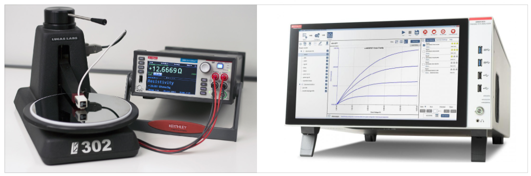
The effort to boost device density and performance while reducing power consumption has led to research into unique two-dimensional (2-D) solids with high carrier mobility and higher conductivity. The desire for greener power generation solutions is spurring investigation into higher temperature superconductors and the power semiconductors essential to power conversion. While the materials of choice today are GaN and SiC, materials research is being conducted on new WBG materials including aluminum nitride (AlN), gallium oxide (Ga2O3), and diamond. These new materials have the potential to unlock even greater power performance. Keithley, a Tektronix company, has led the world in creating some of the most sensitive test and measurement instrumentation, including its line of graphical source measure unit (SMU) instruments and semiconductor parameter analyzers for making resistivity and Hall effect and mobility measurements, enabling researchers, scientists and engineers to unlock the potential of new WBG materials.
Characterization of Wide Bandgap Devices
Understanding the electrical performance of SiC and GaN will help enable a strong value proposition for their use in emerging power applications. To achieve this, current versus voltage (I-V) characterization is performed.
I-V characterization is a fundamental method of understanding the current versus voltage relationship of silicon, silicon carbide and gallium nitride’s fundamental properties. Using instruments like SMUs or parameter analyzers and appropriate software, an I-V graphical curve is generated that is used to show the relationship between the current flowing through an electronic device or circuit and the applied voltage across its terminals.
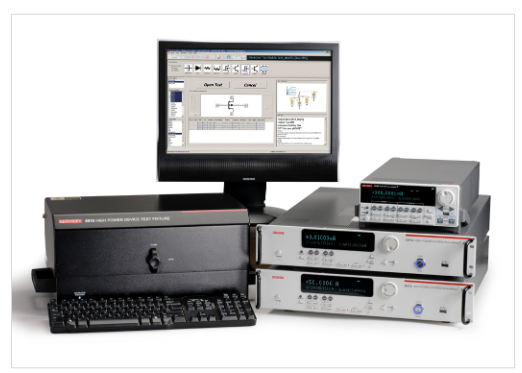
Keithley’s line of 2400 Series Graphical SMUs, the 4200A-SCS Parameter Analyzer and the 2600-PCT High Power I-V Curve Tracer Systems minimize the learning curve for the engineer to help them get their power semiconductor devices to market faster. Many of the key measurements for characterizing WBG devices such as current vs. voltage testing, breakdown voltage testing and leakage current testing are available right at your fingertips through the graphical user interfaces or through application software such as Keithley KickStart or ACS-Basic.
Double Pulse Testing
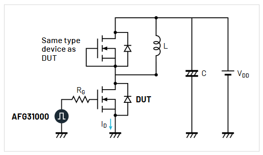
Minimizing switch losses continues to be a major challenge for power device engineers. These designs must be rigorously measured to ensure compliance. The standard test method for measuring switching parameters and evaluating the dynamic behavior of Si, SiC and GaN MOSFETs and IGBTs is the double pulse test (DPT). Double pulse testing is used to measure energy loss during device turn-on and turn-off, as well as reverse recovery parameters.
The double pulse test is performed using two WBG devices. One device is the device under test (DUT) and the second device is typically the same type of device as the DUT. Note the inductive load on the “high” side device. The inductor is used to replicate circuit conditions that you may have in a converter design.
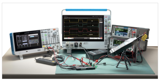
The instruments used include a power supply or SMU to supply the voltage, an arbitrary function generator (AFG) to output pulses that trigger the gate of the MOSFET to turn it on to start conduction of the current and an oscilloscope to measure the resulting waveforms.
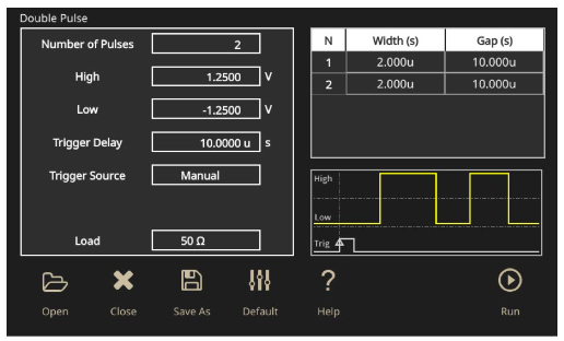
Historically, it has been a time-consuming process to set up because function generators do not usually have a builtin way to configure and set up the test. Newer AFGs like the Tektronix AFG31000 Series include a built-in software application that enables DPT right from the touchscreen interface of the instrument, dramatically simplifying the process for engineers.
Validation of Wide Bandgap Devices
The ability to analyze power loss and optimize power supply efficiency is more critical than ever. One of the key factors in efficiency is the loss in switching devices. For example, a typical switch-mode power supply might have an efficiency of about 87%, meaning that 13% of the input power is dissipated within the power supply, mostly as waste heat. Of this loss, a significant portion is dissipated in the switching devices, usually MOSFETs or IGBTs. Tektronix makes it easy with the 5 and 6 Series B MSO oscilloscopes and automated power analysis software to make switching loss measurements.
Floating differential measurements (such as high-side Vgs) are difficult or impossible to make due to high frequency (fast turn on and turn off) and the presence of high common mode voltages (such as Vds) because oscilloscope probes do not have sufficient common mode rejection at high bandwidth. The poor common mode rejection leads to the measurement being dominated by the common mode error instead of the actual differential signal. These issues can be easily resolved using Tektronix IsoVu™ isolated probes that do not de-rate with frequency at the operating requirements of GaN and SiC devices, allowing you to make accurate differential measurements. With IsoVu probes, you can precisely calculate and prove conduction losses, dead time losses and switching losses.
Conclusion
We live in a changing world where the management of limited energy resources has become more critical. Advances in wide bandgap semiconductor technology like silicon carbide and gallium nitride are enabling the development of a clean, renewable and reliable energy ecosystem while creating new challenges for engineers. Testing tools and techniques of old will simply not be sufficient; without the ability to measure critical values and ensure the functionality of important devices, our progress can only go so far. Researchers and engineers count on Tektronix and Keithley to provide the measurement solutions to address today’s electrified ecosystem challenges and those to come.
To learn more about the four key focus areas discussed in this primer, click on the links below:
- EV Battery Testing
- Wide Bandgap Semiconductor Materials Research
- Characterization of Wide Bandgap Devices
- Double Pulse Testing
- Validation of Wide Bandgap Devices
Find more valuable resources at TEK.COM
Copyright © Tektronix. All rights reserved. Tektronix products are covered by U.S. and foreign patents, issued and pending. Information in this publication supersedes that in all previously published material. Specification and price change privileges reserved. TEKTRONIX and TEK are registered trademarks of Tektronix, Inc. All other trade names referenced are the service marks, trademarks or registered trademarks of their respective companies.
011724 1KW-74060-0