联系我们
与泰克代表实时聊天。 工作时间:上午 9:00 - 下午 5:00(太平洋标准时间)。
电话
致电我们
工作时间:上午9:00-下午5:00(太平洋标准时间)
下载
下载手册、产品技术资料、软件等:
反馈
材料科学—泰克材料电学特性参数测试方案
释放新材料的潜力
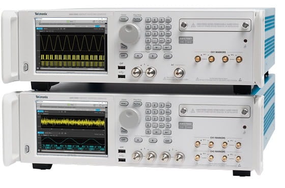
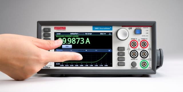
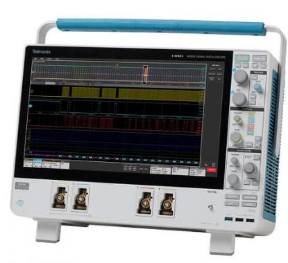
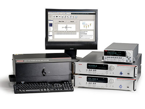
泰克及旗下吉时利品牌,提供各类材料电参数测试方案,包括:
- 电输运特性测试,量子材料、超导材料、半金属材料、异质结构材料,物性表征测试方案
- 新一代高速存储单元及类脑计算、神经元网络测试方案:
- 相变材料及器件电学表征测试方案
- 忆阻器单元基础研究测试方案
- 忆阻器单元性能研究测试方案
- 低维神经元网络阵列测试方案
- 三端器件节点神经元网络阵列测试方案
- 神经元网络阵列测试方案
- 神经形态计算器件和阵列测试解决方案
- 铁电材料及铁电电子器件电学表征
- 自旋电子学 - 电输运表征及器件测试
- 微机电系统MEMS 测试方案
- 宽禁带半导体材料及功率半导体器件测试方案
- 碳基半导体材料及电子器件测试方案
- 基于FET 结构的生物传感器(BioFET) 测试方案
- 有机半导体材料及有机电子器件电性能测试方案
- 柔性半导体材料及电子器件电性能测试方案
- 薄膜类及表面材料的电阻率测试方案
- 绝缘材料电性能表征测试方案
- 使用电压斜坡和电流斜坡技术评估氧化物可靠性方案
材料测试平台主要提供材料电学特性的测试方案。电学特性是许多材料研究的重点,常见的测试参数:
- 包括电阻率,方阻,载流子浓度,载流子迁移率等
- 常用的测试方法是四探针法,范德瓦尔堡法,霍尔效应。
半导体材料与器件科学云讲堂
帮助您理解新一代半导体材料的特性和实际应用,以及其测试痛点
实际半导体材料的特性及实际应用:
-
基于JEDEC标准测试SiC MOSFET的阈值电压
直播回放 讲义下载 白皮书下载 -
芯片物料表征与可靠性测试
直播回放 讲义下载 -
超宽禁带氧化镓功率器件的应用与发展
直播回放 讲义下载 -
OFET&Display 电学性能参数测试
直播回放 讲义下载 白皮书下载 -
超低电容(fF)测试
直播回放 讲义下载 白皮书下载 -
钙钛矿光伏应用测试与表征
直播回放 讲义下载 白皮书下载 -
高耐久性氧化铪基铁电晶体管器件与应用
直播回放 讲义下载 -
范德堡和霍尔测试
直播回放 讲义下载 白皮书下载 -
HOT_CARRIER_热不热
直播回放 讲义下载 白皮书下载 -
半导体参数分析仪4200A自定义软件解决方案
直播回放 讲义下载 -
大模型时代的存算一体芯片
直播回放 讲义下载 -
OLED电学参数测试详解
直播回放 讲义下载 -
MOSFET电容测试方案
直播回放 讲义下载 白皮书下载 -
如何测量 MOSFET 栅极电荷
直播回放 讲义下载 白皮书下载 -
如何进行晶圆级可靠性测试
直播回放 讲义下载 晶圆白皮书 HCI&电迁移 -
薄膜材料电阻率与霍尔迁移率测试详解
直播回放 讲义下载 -
宽禁带半导体材料及功率半导体器件测试
直播回放 讲义下载 -
半导体可靠性热载流子效应测试详解
直播回放 讲义下载 -
1/f噪声测试方案详解
直播回放 讲义下载 -
忆阻器的发展及测试方案
直播回放 讲义下载 -
深度解析IV与CV参数测试难题
直播回放 讲义下载 -
碳基及宽禁带半导体材料与电子器件测试方案
直播回放 讲义下载 -
忆阻器存算一体芯片与类脑计算
直播回放 讲义下载 -
宽禁带半导体器件静态测试规范解读:
直播回放 讲义下载 -
基于FET结构的生物传感器测试:
直播回放 讲义下载 -
材料科学电学性能研究中几种特殊应用案例分享:
直播回放 讲义下载 -
纳米材料及纳米电子器件IV和CV测试:
直播回放 讲义下载 Q&A -
二维材料/石墨烯及其电子器件IV和CV测试:
直播回放 讲义下载